Do you have a question about the Abov A96G166 and is the answer not in the manual?
Lists other documents and resources relevant to the product.
Details the core features and peripheral counts of the device.
Illustrates the pin configuration for various package types.
Lists and explains the function of each pin for different packages.
Details the registers controlling I/O port direction, pull-ups, and open-drain behavior.
Describes the layout and addressing of the on-chip flash program memory.
Details the internal RAM, SFR, and external XRAM spaces.
Describes the XRAM and XSFR memory areas.
Provides a summary and detailed mapping of Special Function Registers.
Covers Px, PxIO, PxPU, PxOD, PxDB, PxFSR registers.
Details the P0, P1, P2, and P3 ports including their registers and function selection.
Details the configuration and operation of external interrupt pins.
Provides a visual representation of the interrupt controller's internal logic.
Lists all interrupt sources, their priorities, and vector addresses.
Illustrates the internal structure of the clock generator.
Lists the registers used for configuring the clock generator.
Shows the block diagram of the Basic Interval Timer.
Lists the registers associated with the BIT.
Explains how to configure the watchdog timer's window period.
Provides a block diagram illustrating the Watchdog Timer's operation.
Shows the block diagram of the Watch Timer.
Lists the registers used for controlling the Watch Timer.
Details the features, modes, and registers of Timer 0.
Details the features, modes, and registers of Timer 1.
Details the features, modes, and registers of Timer 2.
Illustrates the block diagram of the buzzer driver circuit.
Describes the timing requirements for ADC conversion.
Illustrates the block diagram of the ADC module.
Explains the steps and flow for performing an ADC conversion.
Covers I2C block diagram, bit transfer, start/stop, data transfer, acknowledge, and arbitration.
Details I2C initialization, interrupt service, master transmitter, and slave receiver operations.
Covers block diagram, clocking, modes, data format, parity, and transmitter/receiver basics.
Details receiver flags, SPI mode, RTO, and USART register descriptions.
Shows the block diagram of the CRC module.
Lists the registers for configuring and controlling the CRC module.
Details how peripherals behave in IDLE and STOP power-down modes.
Explains how to enter and exit the IDLE power-down mode.
Details entering STOP mode and its release conditions.
Covers reset sources, block diagram, and external reset input.
Details POR, LVR, LVI, registers, and timing related to reset.
Covers registers for controlling and monitoring flash memory operations.
Describes the overall memory map, including flash memory organization.
Explains the Serial In-System Programming (ISP) method and flash operations.
Details how to enter the In-System Programming (ISP) mode.
Explains security features like lock bits and password protection.
Describes how to configure device options using specific registers.
Details the password protection mechanism for device access.
Lists the limits beyond which device damage may occur.
Specifies the voltage and temperature ranges for reliable operation.
Covers ADC, voltage references, reset, oscillators, DC, AC, USART, SPI, I2C, flash, and package characteristics.
Provides dimensional drawings for various package types (SOPN, TSSOP, SOP, QFN, LQFP).
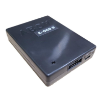
Recommends compilers and details the On-Chip Debugger (OCD) system.
Covers programmers (E-PGM+, E-Gang), flash programming, and the OCD interface.
Lists available part numbers with their features and package types.
Lists the available CPU instructions with their mnemonics, bytes, cycles, and hex codes.
| Brand | Abov |
|---|---|
| Model | A96G166 |
| Category | Computer Hardware |
| Language | English |