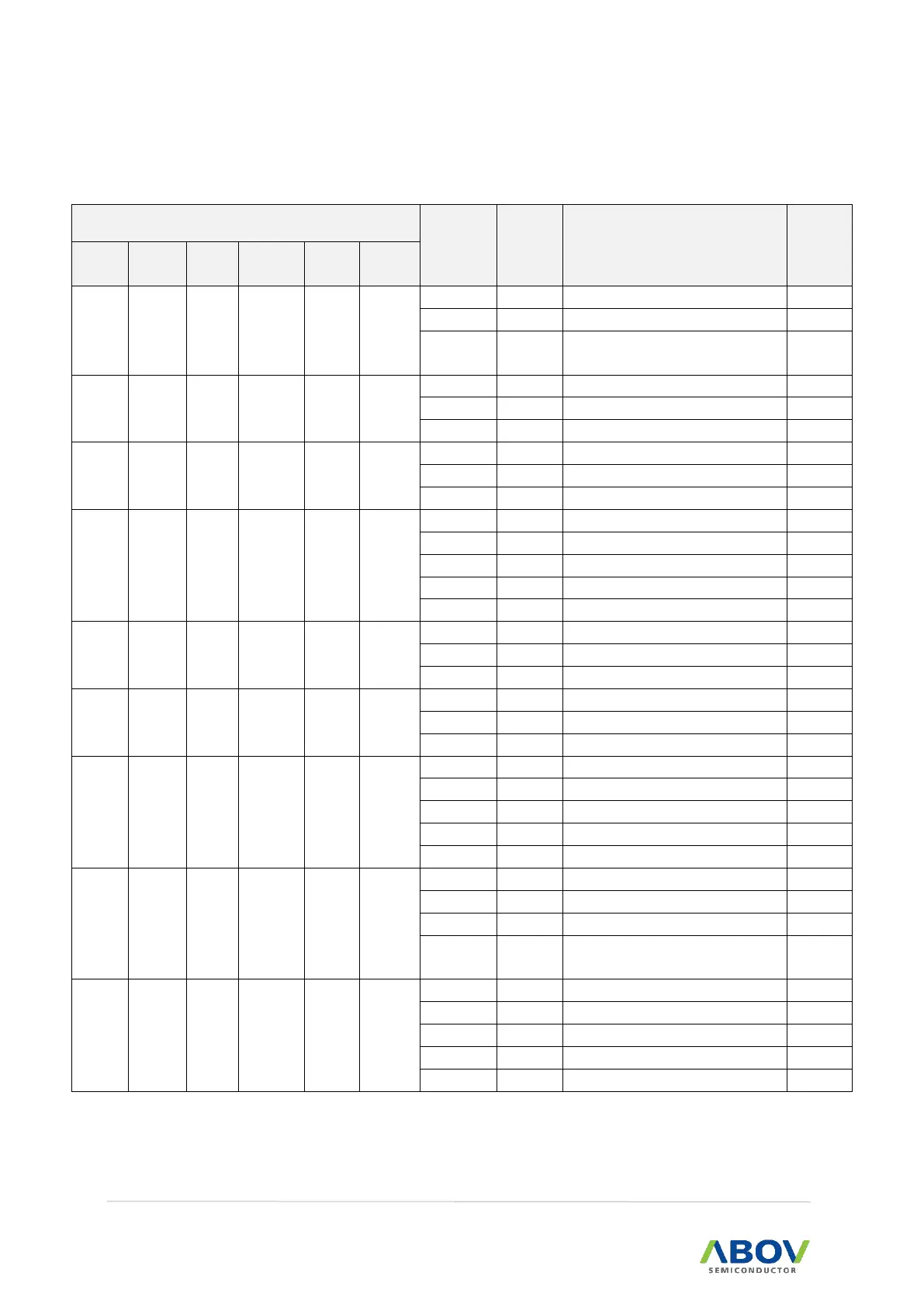
2. Pinouts and pin description A96G166/A96A166/A96S166 User’s manual
2.2 Pin description
Table 2. Normal Pin Description
Port 0 bit 0 Input/output
OCD debugger data
input/output
Port 0 bit 1 Input/output
Port 0 bit 2 Input/output
External interrupt input ch-0
Port 0 bit 3 Input/output
External interrupt input ch-1
Port 0 bit 4 Input/output
External interrupt input ch-2
Port 0 bit 5 Input/output
External interrupt input ch-3
Port 0 bit 6 Input/output
External interrupt input ch-4
Port 1 bit 0 Input/output
External interrupt input ch-5
Timer 1 PWM complementary
output
Port 1 bit 1 Input/output
External interrupt input ch-6
Timer 1(Event Capture) input