EasyManuals Logo

Abov A96G166 User Manual

Default Icon
247 pages
To Next Page IconTo Next Page
To Previous Page IconTo Previous Page
Page #22 background imageLoading...
Page #22 background image
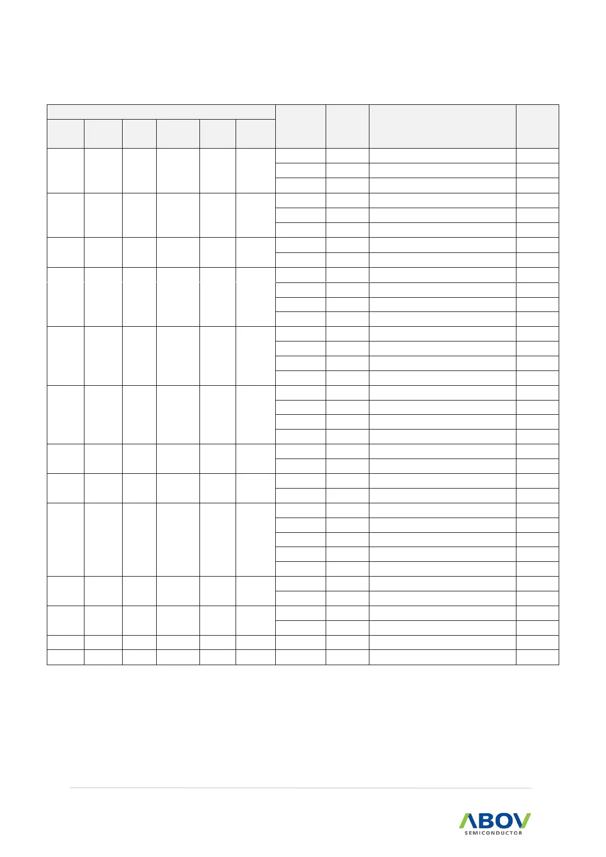
2. Pinouts and pin description A96G166/A96A166/A96S166 User’s manual
22
Table 2. Normal Pin Description (continued)
Pin no.
PIN name
I/O(1)
Description
Remark
32
LQFP
28
SOP
24
QFN
20
TSSOP
20
SOP
16
SOPN
9
11
8
9
(9)
9
7
P24*
IOU
Port 2 bit 4 Input /output
SDA
IO
I2C data signal
TXD1
O
USART1 data transmit
8
10
7
8
(8)
8
6
P25*
IOU
Port 2 bit 5 Input /output
SCL
IO
I2C clock signal
RXD1
I
USART1 data receive
7
-
-
-
-
5
P26*
IOU
Port 2 bit 6 Input /output
EC0
I
Timer 0(Event Capture) input
6
9
6
7
(7)
7
-
P30*
IOUS
Port 3 bit 0 Input /output
TXD1
O
USART1 data transmit
EC2
I
Timer 2(Event Capture) input
SDA
IO
I2C data signal
5
8
5
6
(6)
6
-
P31*
IOUS
Port 3 bit 1 Input /output
RXD1
I
USART1 data receive
EC0
I
Timer 0(Event Capture) input
SCL
IO
I2C clock signal
4
7
4
5
(5)
5
4
P32*
IOUS
Port 3 bit 2 Input /output
RESETB
IU
A96G166 only, Reset pin
Pull-up
T0O
O
Timer 0 interval output
PWM0O
O
Timer 0 PWM output
3
6
3
-
-
-
P33*
IOUS
Port 3 bit 3 Input /output
SXOUT
O
Sub Oscillator Output
2
5
2
-
-
-
P34*
IOUS
Port 3 bit 4 Input /output
SXIN
I
Sub Oscillator Input
1
4
1
4
(4)
4
-
P35*
IOUS
Port 3 bit 5 Input /output
EINT10
I
External interrupt input ch-10
T0O
O
Timer 0 interval output
PWM0O
O
Timer 0 PWM output
RESETB
IU
A96S166 only, Reset pin
Pull-up
32
3
24
3
(3)
3
3
P36*
IOUS
Port 3 bit 6 Input/output
XIN
I
Main Oscillator Input
31
2
23
2
(2)
2
2
P37*
IOUS
Port 3 bit 7 Input/output
XOUT
I
Main Oscillator Output
29
28
21
20
(1)
20
16
VDD
P
VDD
30
1
22
1
(20)
1
1
VSS
P
VSS
NOTES:
1. The
(*)
is applied to 20 TSSOP of A96S166
2. The P04–P06 and P26 are not in the 28-pin package.
3. The P04–P06, P17, P20-P22 and P26 are not in the 24-pin package.
4. The P04–P06, P14-P17, P20, P23, P26 and P33-P34 are not in the 20-pin package.
5. The P02-P05, P10-P11, P16-P17, P20-P21, P23, P30-P31 and P33-P35 are not in the 16-pin package.
6. The P32/RESETB (A96G166) pin is configured as one of the P32 and RESETB pin by the
“CONFIGURE OPTION.” (P35/RESETB : A96S166)
7. If the P00/AN0/DSDA and P01/AN1/DSCL pins are connected to the programmer during power-on
reset, the pins are automatically configured as In-system programming pins.

Table of Contents

Questions and Answers:

Question and Answer IconNeed help?

Do you have a question about the Abov A96G166 and is the answer not in the manual?

Abov A96G166 Specifications

General IconGeneral
BrandAbov
ModelA96G166
CategoryComputer Hardware
LanguageEnglish

Related product manuals