4. Memory organization A96G166/A96A166/A96S166 User’s manual
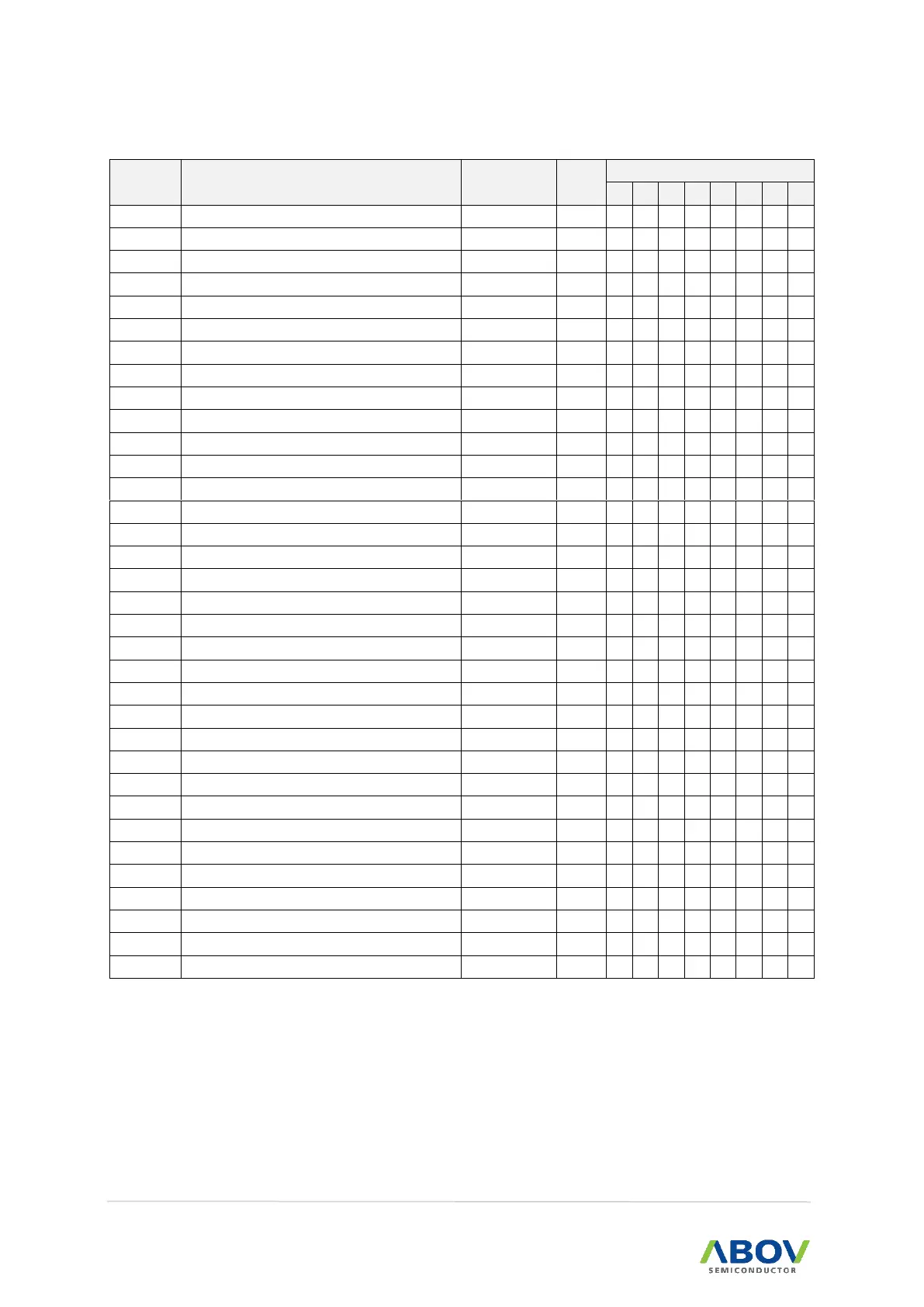
Table 5. SFR Map (continued)
External Interrupt Flag 0 Register
Timer 2 Control Low Register
Timer 2 Control High Register
Timer 2 A Data Low Register
Timer 2 A Data High Register
Timer 2 B Data Low Register
Timer 2 B Data High Register
Oscillator Control Register
USART0 Control Register 1
USART0 Control Register 2
USART0 Control Register 3
USART0 Baud Rate Generation Register
Program Status Word Register
P0 Function Selection Low Register
P0 Function Selection High Register
P1 Function Selection Low Register
P1 Function Selection High Register
P2 Function Selection Low Register
P2 Function Selection High Register
Low Voltage Reset Control Register
P0 De-bounce Enable Register
P1 De-bounce Enable Register
I2C Mode Control Register
I2C Slave Address Register
I2C Slave Address Register 1