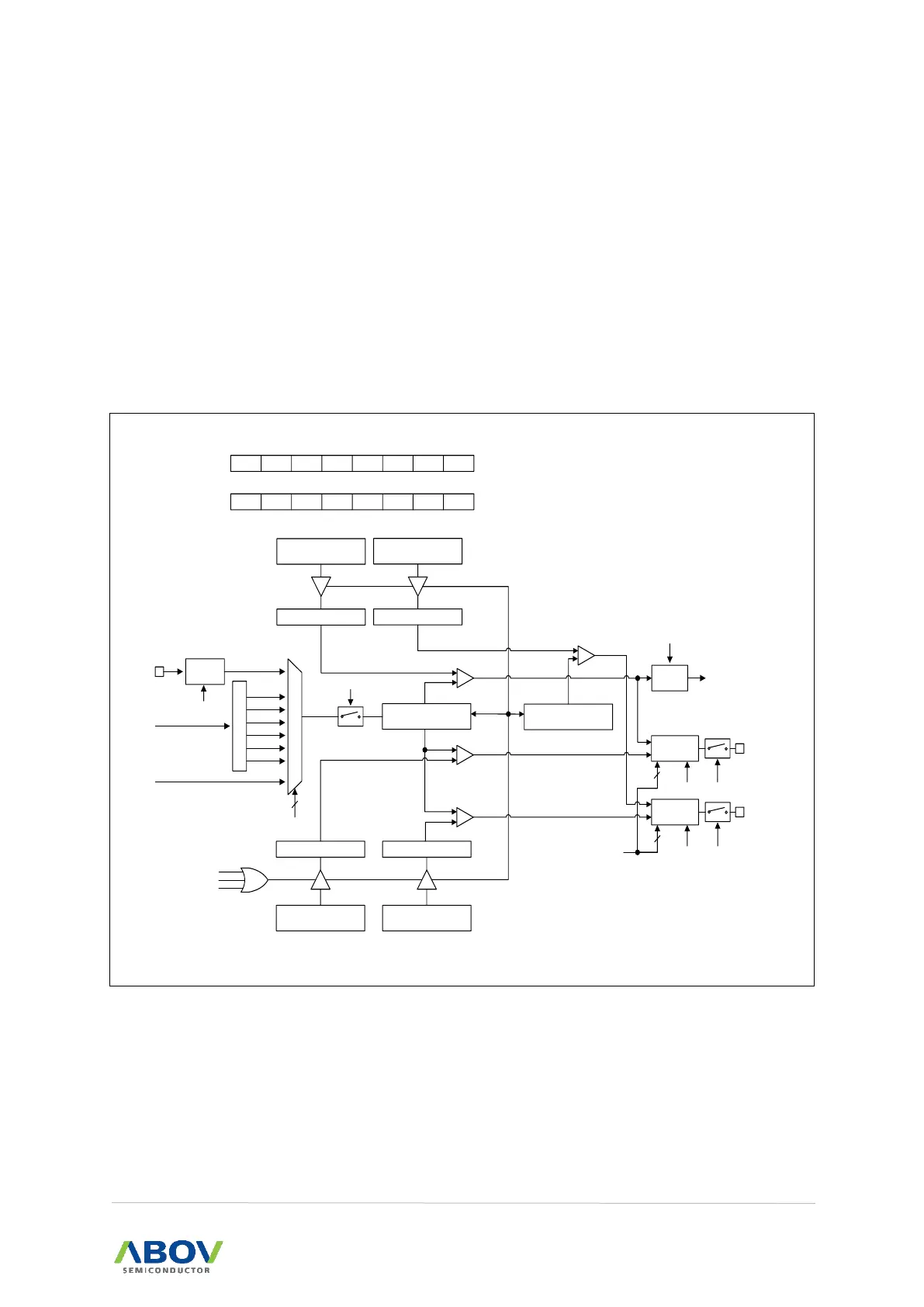
11.2.4 16-bit complementary PWM mode (dead time)
The timer 1 has a complementary PWM function. The complementary PWM output function operates
when T1BEN is set. In PPG mode, PWM1O/PWM1OB pin outputs up to 16-bit resolution
complementary PWM output. This pin should be configured as a PWM output by setting P1FSRL[1:0]
to ‘01’.
The period of the PWM output is determined by the T1ADRH/T1ADRL. And the duty of the PWM
output is determined by the T1BDRH/T1BDRL. The delay (dead time) of the Complementary PWM
output is determined by T1CDRH / T1CDRL. And the duty of the Complementary PWM output is
determined by T1DDRH / T1DDRL.
T1MS[1:0]
T1POL
Reload
P
r
e
s
c
a
l
e
r
fx
M
U
X
fx/2
fx/4
fx/64
fx/2048
fx/8
fx/1
Comparator
16-bit Counter
T1CNTH/T1CNTL
16-bit B Data Register
T1BDRH/T1BDRL
Clear
B Match
Edge
Detector
T1ECE
EC1
Buffer Register B
Comparator
16-bit A Data Register
T1ADRH/T1ADRL
T1IFR
INT_ACK
Clear
To interrupt
block
A Match
Buffer Register A
Reload
Pulse
Generator
PWM1O
R
T1EN
3
T1CK[2:0]
2
T1EN
T1CRH
1
ADDRESS:BBH
INITIAL VALUE : 0000_0000B
T1BEN T1MS1 T1MS0
– –
T1PE T1CC
1 1 1
– –
1 X
T1CK2
T1CRL
X
ADDRESS:BAH
INITIAL VALUE : 0000_0000B
T1CK1 T1CK0 T1IFR T1BPOL T1POL T1ECE T1CNTR
X X X X X X X
T1PE
A Match
T1CC
T1EN
16-bit C Data Register
T1CDRH/T1CDRL
Buffer Register C
T1BPOL
Pulse
Generator
PWM1OB
2
T1BEN
C Match
Reload
16-bit Counter
TZCNTH/TZCNT
16-bit D Data Register
T1DDRH/T1DDRL
Buffer Register D
Reload
R
D Match
HSIRC