MPC5200B Users Guide, Rev. 1
2-6 Freescale Semiconductor
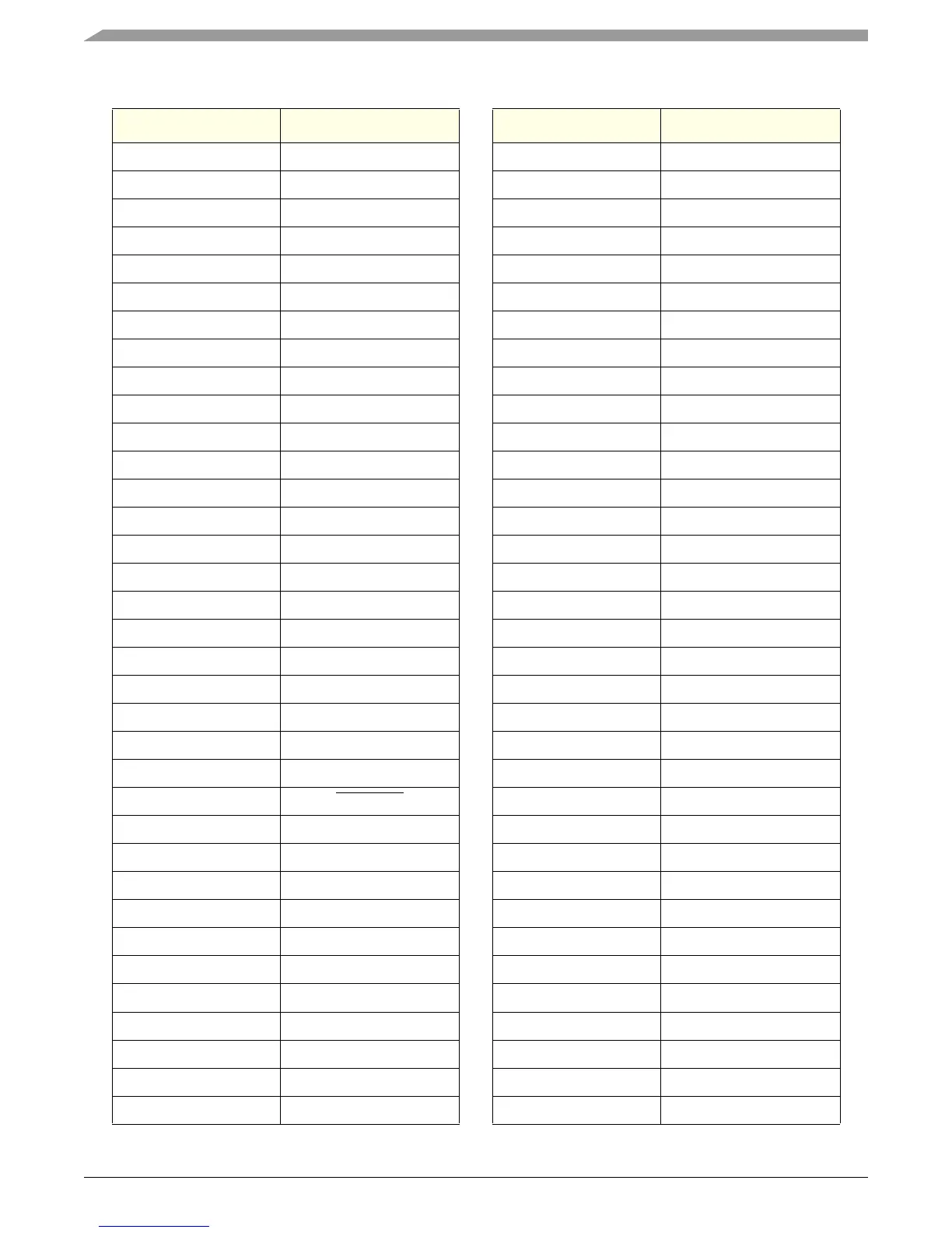
Pinout Tables
E01 TIMER_7 J10 VSS_IO/CORE
E02 TIMER_6 J11 VSS_IO/CORE
E03 TIMER_5 J12 VSS_IO/CORE
E04 VDD_IO J17 MEM_MDQ_22
E17 VDD_MEM_IO J18 MEM_MDQ_21
E18 MEM_MDQ_16 J19 MEM_MDQ_8
E19 MEM_MA_9 J20 MEM_MDQ_9
E20 MEM_MA_11 K01 ETH_0
F01 USB_7 K02 ETH_1
F02 USB_8 K03 ETH_2
F03 USB_9 K04 VDD_CORE
F04 VDD_IO K09 VSS_IO/CORE
F17 VDD_MEM_IO K10 VSS_IO/CORE
F18 MEM_MDQ_17 K11 VSS_IO/CORE
F19 MEM_MA_12 K12 VSS_IO/CORE
F20 MEM_CLK_EN K17 VDD_MEM_IO
G01 USB_3 K18 MEM_MDQ_23
G02 USB_4 K19 MEM_MDQ_10
G03 USB_5 K20 MEM_MDQ_11
G04 USB_6 L01 ETH_9
G17 MEM_MDQ_18 L02 ETH_16
G18 MEM_MDQ_19 L03 ETH_5
G19 MEM_CLK L04 ETH_11
G20 MEM_CLK
L09 VSS_IO/CORE
H01 USB_0 L10 VSS_IO/CORE
H02 USB_1 L11 VSS_IO/CORE
H03 USB_2 L12 VSS_IO/CORE
L17 MEM_DQM_3 R18 MEM_MDQ_29
L18 MEM_MDQS_3 R19 MEM_MDQ_5
L19 MEM_MDQ_12 R20 MEM_MDQ_4
L20 MEM_MDQ_13 T01 PCI_CLOCK
M01 ETH_13 T02 EXT_AD_26
M02 ETH_12 T03 EXT_AD_28
M03 ETH_8 T04 VDD_IO
M04 VDD_CORE T17 VDD_MEM_IO
Table 2-1. Signals by Ball/Pin (continued)
Ball/Pin Pin Name Ball/Pin Pin Name