MB95630H Series
MN702-00009-2v0-E FUJITSU SEMICONDUCTOR LIMITED 253
CHAPTER 14 LIN-UART
14.7 Registers
[bit5:4] LBL[1:0]: LIN synch break length select bits
These bits select the bit length for the LIN synch break generation time.
The LIN synch break length for reception is always 11 bits.
[bit3] SOPE: Serial output pin direct access enable bit*
This bit enables or disables direct writing to the SOT pin.
Setting this bit to "1" when serial data output has been enabled (SMR:SOE = 1) enables direct writing to the
SOT pin.
[bit2] SIOP: Serial I.O pin direct access bit*
This bit controls direct access to the serial I/O pin.
The SIOP bit always returns the value of the SIN pin if read by a normal read instruction.
If direct access to the serial output pin is enabled (SOPE = 1), the value written to this bit is reflected in the
SOT pin.
Note: When the bit manipulation instruction is used, the SIOP bit returns the bit value of the SOT pin in the
read cycle.
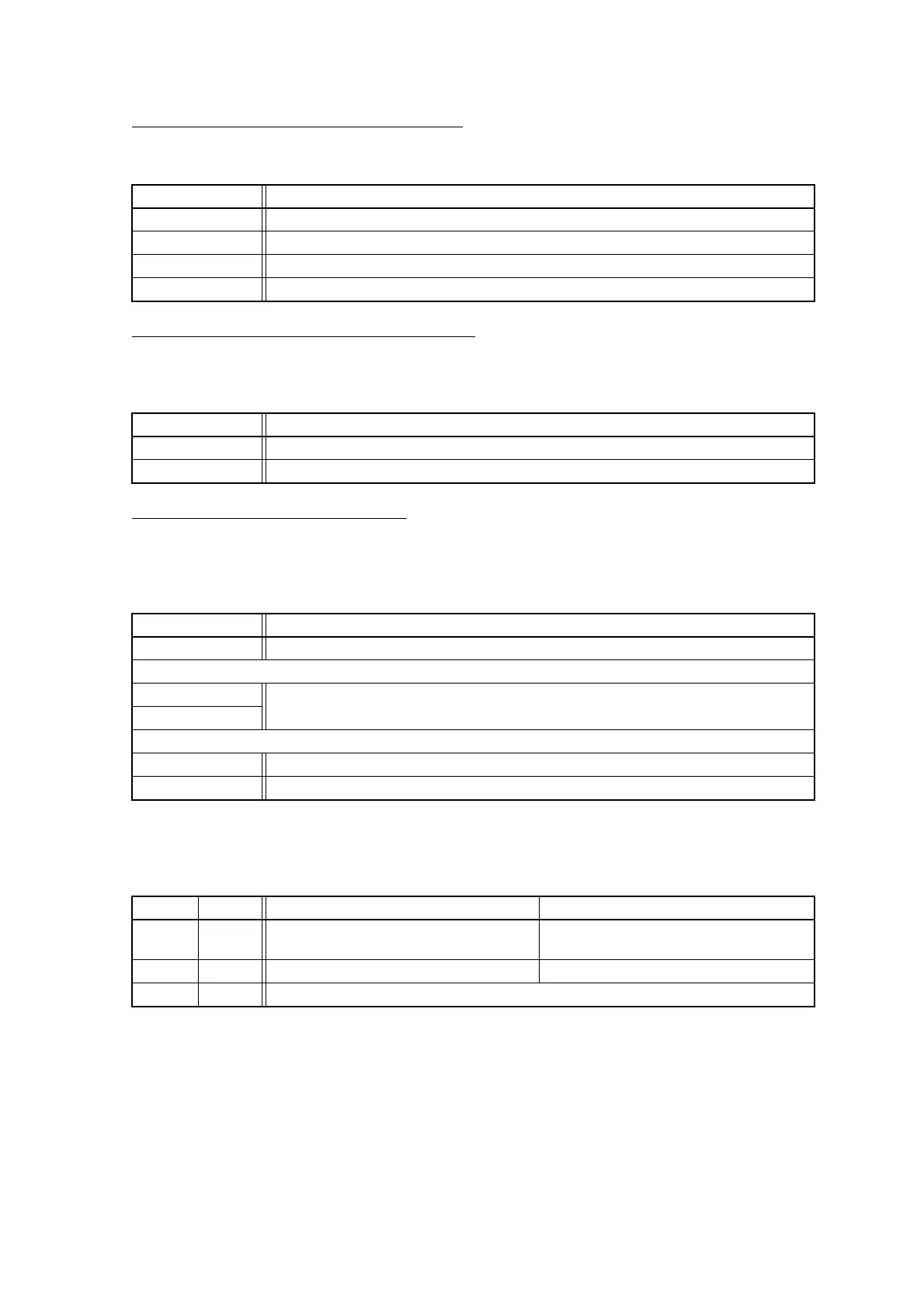
bit5:4 Details
Writing "00" 13 bits
Writing "01" 14 bits
Writing "10" 15 bits
Writing "11" 16 bits
bit3 Details
Writing "0" Disables serial output pin direct access.
Writing "1" Enables serial output pin direct access.
bit2 Details
Read access Reads the value of the SIN pin.
With the SOPE bit set to "0":
Writing "0"
Has no effect on operation.
Writing "1"
With the SOPE bit set to "1":
Writing "0" Fixes the SOT pin at "0".
Writing "1" Fixes the SOT pin at "1".
*: Relationship between SOPE and SIOP
SOPE SIOP Write access to SIOP Read access to SIOP
0 R/W
It has no effect on operation. (However, the
value written to the SIOP bit is held.)
It returns the value of the SIN pin.
1 R/W It writes "0" or "1" to the SOT pin. It returns the value of the SIN pin.
1 RMW It reads the value of the SOT pin and writes "0" or "1" to the SOT pin.