MB95630H Series
MN702-00009-2v0-E FUJITSU SEMICONDUCTOR LIMITED 477
CHAPTER 22 UART/SIO
22.7 Registers
22.7.1 UART/SIO Serial Mode Control Register 1 ch. n
(SMC1n)
The UART/SIO serial mode control register 1 ch. n (SMC1n) controls the UART/
SIO operation mode. The register is used to set the serial data direction
(endian), parity and its polarity, stop bit length, operation mode (clock
synchronous mode / clock asynchronous mode), data length, and serial clock.
■ Register Configuration
■ Register Functions
[bit7] BDS: Serial data direction control bit
This bit controls the serial data direction (endian).
[bit6] PEN: Parity control bit
This bit enables or disables the parity in clock asynchronous mode (UART).
[bit5] TDP: Parity polarity control bit
This bit controls the even/odd parity.
[bit4] SBL: Stop bit length control bit
This bit controls the stop bit length in clock asynchronous mode (UART).
Note: The setting of this bit is only valid for transmission operation in clock asynchronous mode (UART). In
a receive operation, regardless of the setting of this bit, the UART/SIO completes the receive operation
when detecting a stop bit (one bit), and sets the receive data register full flag bit (SSRn:RDRF) to "1".
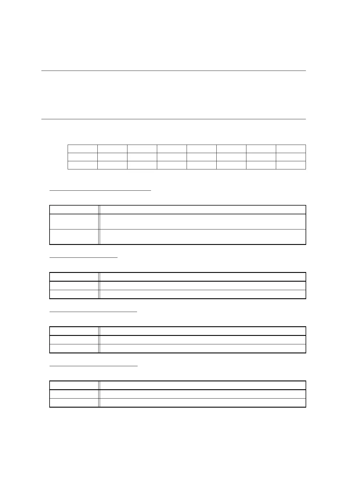
bit 7 6 5 4 3 2 1 0
Field BDS PEN TDP SBL CBL1 CBL0 CKS MD
Attribute R/W R/W R/W R/W R/W R/W R/W R/W
Initial value 0 0 0 0 0 0 0 0
bit7 Details
Writing "0"
Transmission or reception starts from the LSB in the UART/SIO serial input/output data register
ch. n (RDRn/TDRn).
Writing "1"
Transmission or reception starts from the MSB in the UART/SIO serial input/output data register
ch. n (RDRn/TDRn).
bit6 Details
Writing "0" Disables the parity.
Writing "1" Enables the parity.
bit5 Details
Writing "0" Selects the even parity.
Writing "1" Selects the odd parity.
bit4 Details
Writing "0" 1 bit
Writing "1" 2 bits