MB95630H Series
MN702-00009-2v0-E FUJITSU SEMICONDUCTOR LIMITED 275
CHAPTER 15 8/10-BIT A/D CONVERTER
15.6 Registers
15.6.2 8/10-bit A/D Converter Control Register 2 (ADC2)
The 8/10-bit A/D converter control register 2 (ADC2) is used to control different
functions of the 8/10-bit A/D converter, select the input clock, and enable and
disable interrupts.
■ Register Configuration
■ Register Functions
[bit7] AD8: Precision select bit
This bit selects the resolution of A/D conversion.
Writing "0" to this bit selects10-bit precision.
Writing "1" to this bit selects 8-bit precision. Reading the ADDL register can obtain 8-bit data.
Note: The data bits to be used are different depending on the resolution selected. Modify this bit only when
the A/D converter has stopped operating.
[bit6:5] TIM[1:0]: Sampling time select bits
These bits select the sampling time.
Modify the sampling time according to operating conditions (voltage and frequency).
The CKIN value is determined by the clock select bits (ADC2:CKDIV[1:0]).
Note: Modify these bits only when the A/D converter has stopped operating.
[bit4] ADCK: External start signal select bit
This bit selects the start signal for external start (ADC2:EXT = 1).
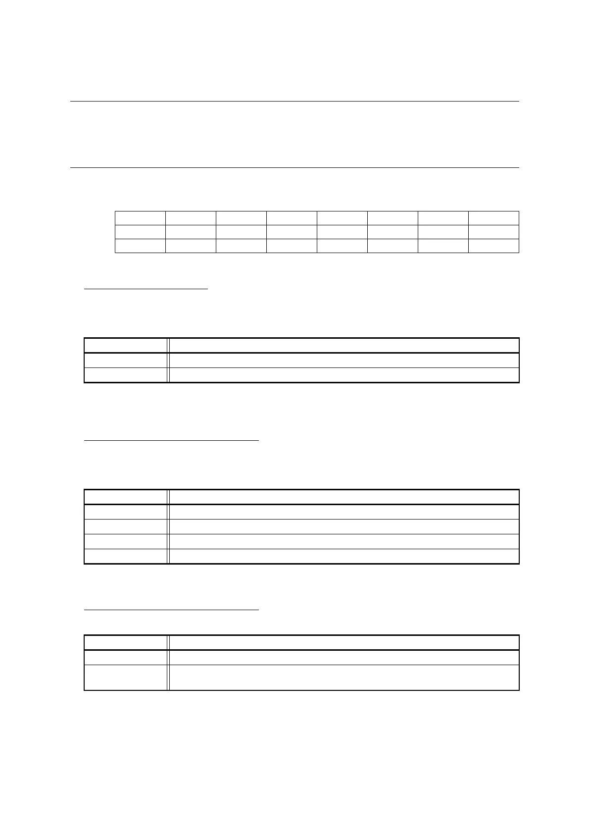
bit 7 6 5 4 3 2 1 0
Field AD8 TIM1 TIM0 ADCK ADIE EXT CKDIV1 CKDIV0
Attribute R/W R/W R/W R/W R/W R/W R/W R/W
Initial value 0 0 0 0 0 0 0 0
bit7 Details
Writing "0" 10-bit precision
Writing "1" 8-bit precision
bit6:5 Details
Writing "00" CKIN × 4
Writing "01" CKIN × 7
Writing "10" CKIN × 10
Writing "11" CKIN × 16
bit4 Details
Writing "0" Selects not using any external start signal to start the A/D conversion function.
Writing "1"
Selects the 8/16-bit composite timer ch. 0 output pin (TO00) as the pin used to start the A/D
conversion function.