MB95630H Series
MN702-00009-2v0-E FUJITSU SEMICONDUCTOR LIMITED 569
CHAPTER 26 DUAL OPERATION FLASH MEMORY
26.8 Registers
26.8.3 Flash Memory Sector Write Control Register 0
(SWRE0)
The flash memory sector write control register 0 (SWRE0) is installed in the
Flash memory interface and used to set the function of protecting the Flash
memory against spurious writes.
The flash memory sector write control register 0 (SWRE0) has bits for enabling/disabling
programming data into individual sectors (SA0 to SA2). The initial value of each bit is "0",
meaning programming data is disabled. Writing "1" to a bit in SWRE0 enables programming
data into the sector corresponding to that bit. Writing "0" to a bit in SWRE0 prevents data from
being accidentally written into the sector corresponding to that bit. When "0" is written to a bit
in SWRE0, even though "1" is written to that bit afterward, data cannot be programmed into
the sector corresponding to that bit. To re-program the data, execute a reset operation.
Only write data to SWRE0 by the byte. Setting the bits in SWRE0 using the bit manipulation
instruction is prohibited.
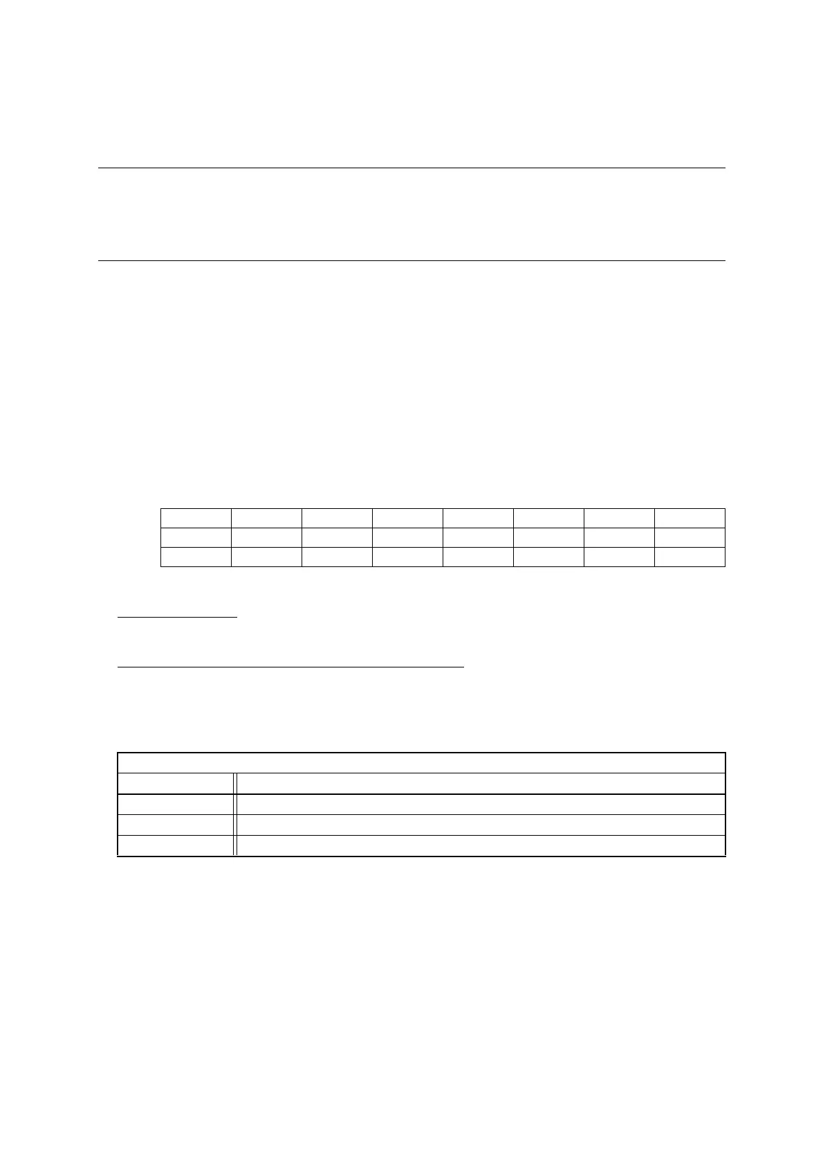
■ Register Configuration
■ Register Functions
[bit7:3] Reserved bits
Always set these bits to "0".
[bit2:0] SA2E, SA1E, SA0E: Programming function setup bits
These bits are used to set the function of preventing data from being accidentally written into a sector of the
Flash memory. Writing "1" to a bit in SWRE0 enables programming data into the sector corresponding to
that bit. Writing "0" to a bit in SWRE0 prevents data from being accidentally written into the sector
corresponding to that bit. In addition, a reset initializes this bit to "0" (programming disabled).
bit 7 6 5 4 3 2 1 0
Field Reserved Reserved Reserved Reserved Reserved SA2E SA1E SA0E
Attribute W W W W W R/W R/W R/W
Initial value 0 0 0 0 0 0 0 0
Table of programming function setup bits and their corresponding Flash memory sectors
Bit name Corresponding sector in Flash memory
SA2E SA2
SA1E SA1
SA0E SA0