MB95630H Series
MN702-00009-2v0-E FUJITSU SEMICONDUCTOR LIMITED 479
CHAPTER 22 UART/SIO
22.7 Registers
22.7.2 UART/SIO Serial Mode Control Register 2 ch. n
(SMC2n)
The UART/SIO serial mode control register 2 ch. n (SMC2n) controls the UART/
SIO operation mode. The register enables or disables serial clock output, serial
data output, transmission/reception, and interrupts, and clears the receive
error flag.
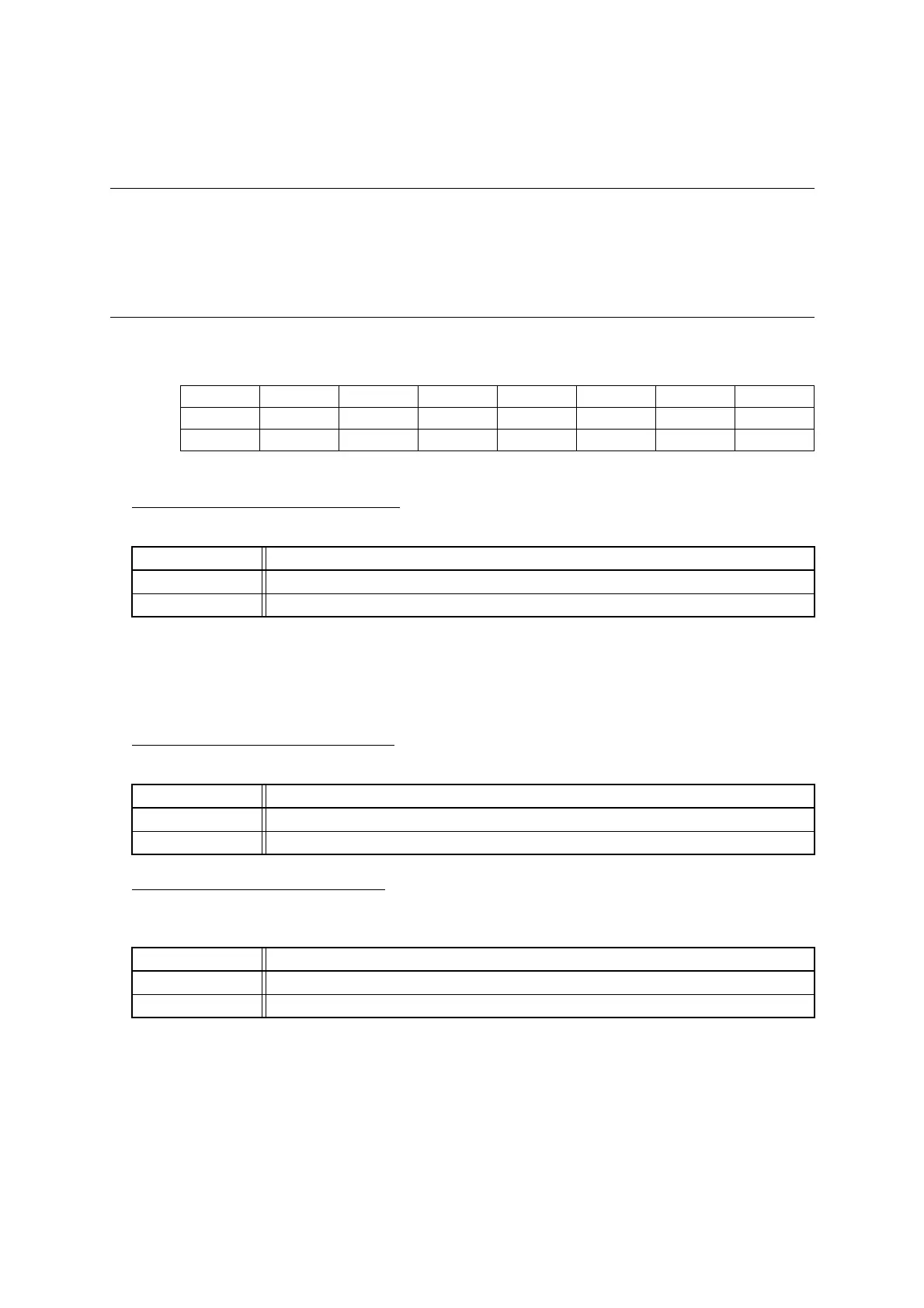
■ Register Configuration
■ Register Functions
[bit7] SCKE: Serial clock output enable bit
This bit controls the input/output of the serial clock pin (UCKn) in clock synchronous mode (SIO).
Note: With the clock select bit (SMC1n:CKS) already set to "1", no internal clock signal is output even
when this bit set to "1".
In clock asynchronous mode (UART) (SMC1n:MD = 0), when this bit is set to "0", the output from
the UCKn bit will always be "H".
[bit6] TXOE: Serial data output enable bit
This bit controls the output of the serial data pin (UOn).
[bit5] RERC: Receive error flag clear bit
This bit clears the receive error flags.
The read value of this bit is always "1".
bit 7 6 5 4 3 2 1 0
Field SCKE TXOE RERC RXE TXE RIE TCIE TEIE
Attribute R/W R/W R/W R/W R/W R/W R/W R/W
Initial value 0 0 1 0 0 0 0 0
bit7 Details
Writing "0" Disables the serial clock, and makes the UCKn pin function as a general purpose I/O port.
Writing "1" Enables the serial clock, and makes the UCKn pin function as a serial clock output pin.
bit6 Details
Writing "0" Disables serial data output, and makes the UOn pin function as a general purpose I/O port.
Writing "1" Enables serial data output, and makes the UOn pin function as a serial data output pin.
bit5 Details
Writing "0" Clears the receive error flags (PER, OVE and FER) in the SSRn register.
Writing "1" Has no effect on operation.