MB95630H Series
32 FUJITSU SEMICONDUCTOR LIMITED MN702-00009-2v0-E
CHAPTER 3 CLOCK CONTROLLER
3.3 Registers
3.3.4 Standby Control Register (STBC)
The standby control register (STBC) controls transition from the RUN state to
sleep mode, stop mode, time-base timer mode, or watch mode, sets the pin
state in stop mode, time-base timer mode, and watch mode, and controls the
generation of software resets.
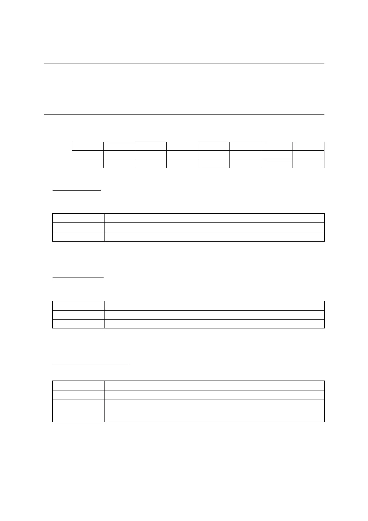
■ Register Configuration
■ Register Functions
[bit7] STP: Stop bit
This bit sets the transition to stop mode.
The read value of this bit is always "0".
Note: After an interrupt request is generated, writing "1" to this bit is ignored. For details, see "3.5.1 Notes
on Using Standby Mode".
[bit6] SLP: Sleep bit
This bit sets the transition to sleep mode.
The read value of this bit is always "0".
Note: After an interrupt request is generated, writing "1" to this bit is ignored. For details, see "3.5.1 Notes
on Using Standby Mode".
[bit5] SPL: Pin state setting bit
This bit sets the states of external pins in stop mode, time-base timer mode, and watch mode.
bit 7 6 5 4 3 2 1 0
Field STP SLP SPL SRST TMD — — —
Attribute W W R/W W W — — —
Initial value 0 0 0 0 0 0 0 0
bit7 Details
Writing "0" Has no effect on operation.
Writing "1" Causes the device to transit to stop mode.
bit6 Details
Writing "0" Has no effect on operation.
Writing "1" Causes the device to transit to sleep mode.
bit5 Details
Writing "0" The state (level) of an external pin in stop mode, time-base timer mode and watch mode is kept.
Writing "1"
An external pin becomes high impedance in stop mode, time-base timer mode and watch mode.
(A pin for which connection to a pull-up resistor has been selected in the pull-up register is pulled
up.)