MB95630H Series
MN702-00009-2v0-E FUJITSU SEMICONDUCTOR LIMITED 325
CHAPTER 18 8/16-BIT PPG
18.7 Registers
18.7.3 8/16-bit PPG timer n1/n0 Cycle Setup Buffer
Register (PPSn1/PPSn0)
The 8/16-bit PPG timer n1/n0 cycle setup buffer register (PPSn1/PPSn0) sets
the PPG output cycle.
■ Register Configuration
■ Register Functions
The PPSn1 and PPSn0 registers set the PPG output cycle.
• In 16-bit PPG mode, PPSn1 serves as the upper 8 bits, while PPSn0 serves as the lower 8
bits.
• In 16-bit PPG mode, write the upper bits before the lower bits. When only the upper bits are
written, the previously written value is reused in the next load.
• 8-bit mode: Cycle = max. 255 (0xFF) × Input clock cycle
• 16-bit mode: Cycle = max. 65535 (0xFFFF) × Input clock cycle
• PPSn1 and PPSn0 are initialized upon reset.
• Do not set the cycle to "0x00" or "0x01" when using the unit in 8-bit PPG independent
mode or 8-bit prescaler mode + 8-bit PPG mode.
• Do not set the cycle to "0x0000" or "0x0001" when using the unit in 16-bit PPG mode.
• If the cycle settings are modified during the operation, the modified settings will be
effective from the next PPG cycle.
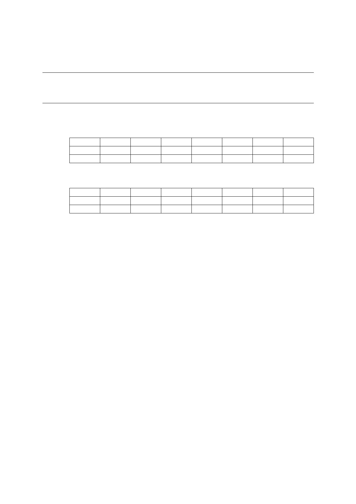
PPSn1
bit 7 6 5 4 3 2 1 0
Field PH7 PH6 PH5 PH4 PH3 PH2 PH1 PH0
Attribute R/W R/W R/W R/W R/W R/W R/W R/W
Initial value 1 1 1 1 1 1 1 1
PPSn0
bit 7 6 5 4 3 2 1 0
Field PL7 PL6 PL5 PL4 PL3 PL2 PL1 PL0
Attribute R/W R/W R/W R/W R/W R/W R/W R/W
Initial value 1 1 1 1 1 1 1 1