MB95630H Series
392 FUJITSU SEMICONDUCTOR LIMITED MN702-00009-2v0-E
CHAPTER 21 MULTI-PULSE GENERATOR
21.5 Operations
21.5 Operations
The operations of the multi-pulse generator will be described in the following
sections. According to the settings of the OPx1 and OPx0 bits in the 16-bit
MPG output data register (upper/lower) (OPDUR/OPDLR), the OPTx pin outputs
the corresponding kind of waveforms ("H" or "L" or PPG output). See Table
21.5-1.
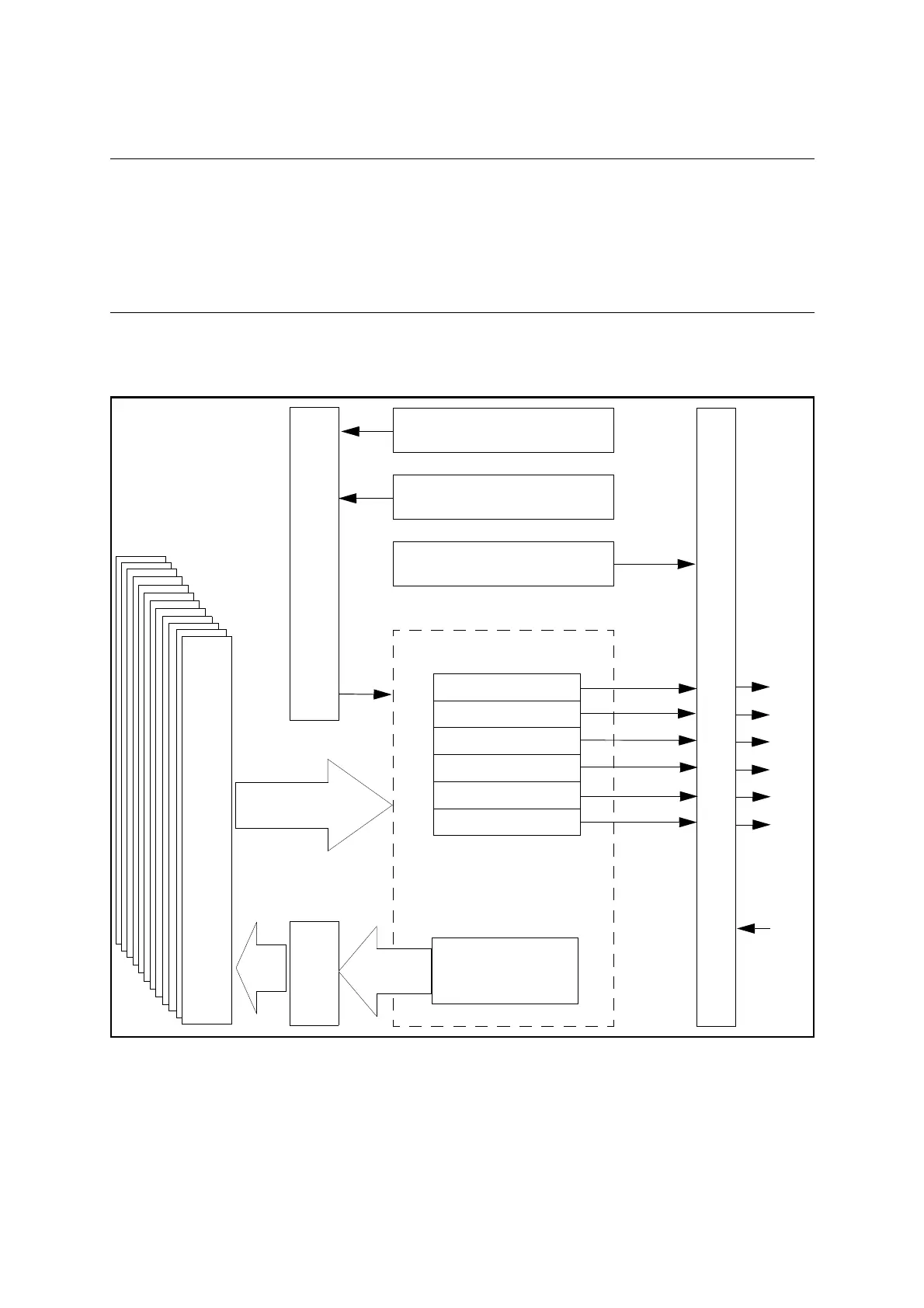
■ Output Data Register Block Diagram
Figure 21.5-1 Output Data Register Block Diagram
OP51/OP50
OP41/OP40
OUTPUT CONTROL CIRCUIT
OPT5
OPT4
OPT3
OPT2
OPT1
OPT0
DTTI
OP31/OP30
OP21/OP20
OP11/OP10
OP01/OP00
BNKF/RDA2
RDA1/RDA0
OUTPUT DATA REGISTER
16-BIT PPG TIMER
DECODER DATA WRITE CONTROL UNIT
POSITION DETECT CIRCUIT
16-BIT RELOAD TIMER
OUTPUT DATA BUFFER REGISTER x 12