MB95630H Series
606 FUJITSU SEMICONDUCTOR LIMITED MN702-00009-2v0-E
CHAPTER 29 SYSTEM CONFIGURATION CONTROLLER
29.2 Register
29.2.1 System Configuration Register (SYSC)
This section describes the system configuration register (SYSC).
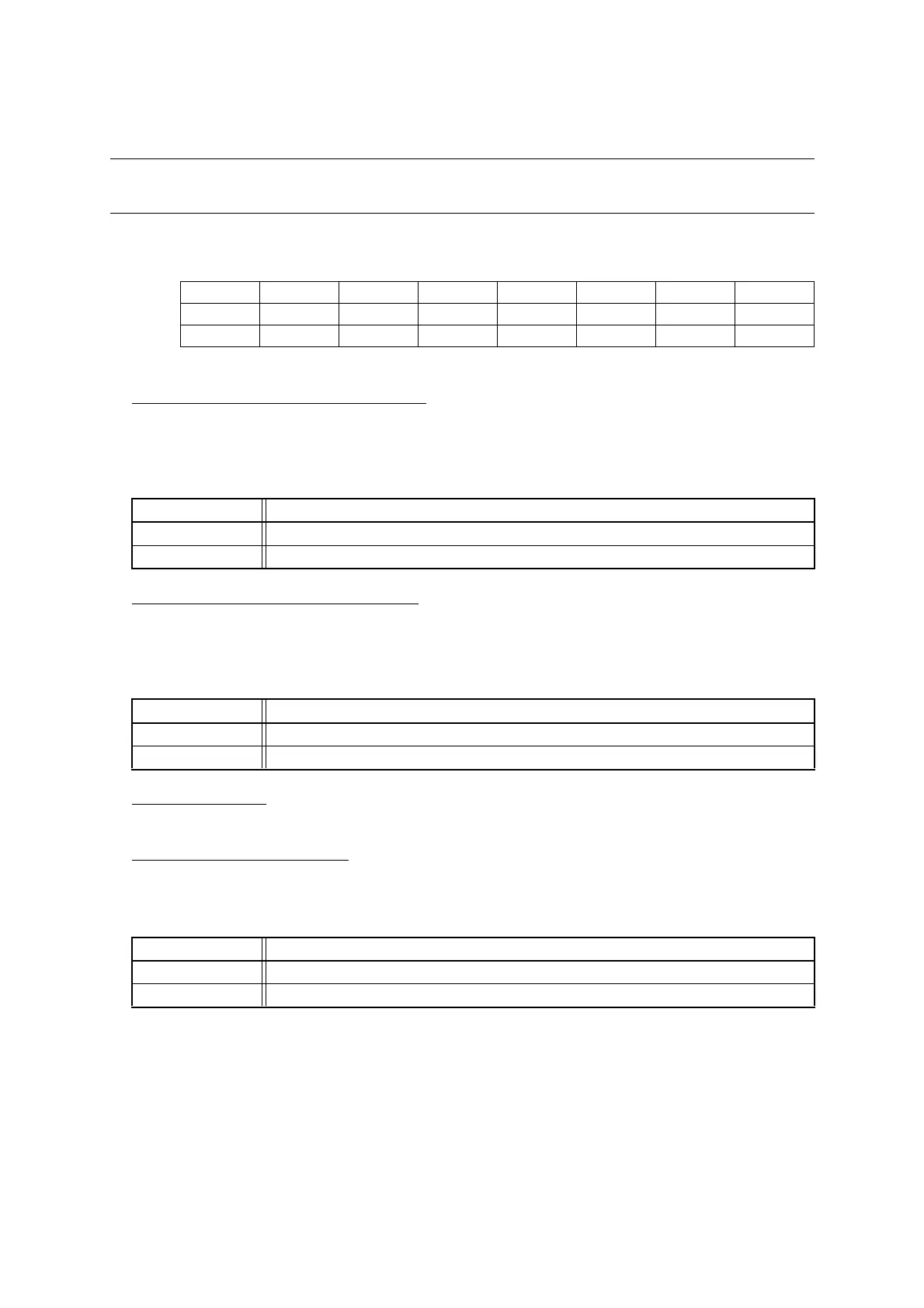
■ Register Configuration
■ Register Functions
[bit7] PGSEL: PG1 and PG2 function select bit
This bit selects the function of the PG1 and PG2 pins.
Writing "0" to this bit makes the PG1 and PG2 pins function as subclock oscillation pins. The subclock
oscillation is enabled or disabled by the subclock oscillation enable bit (SYCC2:SOSCE).
Writing "1" to this bit makes the PG1 and PG2 pins function as general-purpose I/O ports.
[bit6] PFSEL: PF0 and PF1 function select bit
This bit selects the function of the PF0 and PF1 pins.
Writing "0" to this bit makes the PF0 and PF1 pins function as main clock oscillation pins. The main clock
oscillation is enabled or disabled by the main clock oscillation enable bit (SYCC2:MOSCE).
Writing "1" to this bit makes the PF0 and PF1 pins function as general-purpose I/O ports.
[bit5:4] Reserved bits
Always set these bits to "0".
[bit3] EC0SL: EC0 clock select bit
This bit selects the external count clock input pin (EC0) for the 8/16-bit composite timer.
Before using the EC0 input function, enable the external count clock input of the 8/16-bit composite timer.
For details, see "CHAPTER 11 8/16-BIT COMPOSITE TIMER".
bit 7 6 5 4 3 2 1 0
Field PGSEL PFSEL Reserved Reserved EC0SL PPGSEL RSTOE RSTEN
Attribute R/W R/W W W R/W R/W R/W R/W
Initial value 1 1 0 0 0 0 1 1
bit7 Details
Writing "0" Makes the PG1 and PG2 pins function as subclock oscillation pins.
Writing "1" Makes the PG1 and PG2 pins function as general-purpose I/O ports.
bit6 Details
Writing "0" Makes the PF0 and PF1 pins function as main clock oscillation pins.
Writing "1" Makes the PF0 and PF1 pins function as general-purpose I/O ports.
bit3 Details
Writing "0" Selects P12/EC0 pin as the external count clock input pin.
Writing "1" Selects P04/EC0 pin as the external count clock input pin.