MB95630H Series
36 FUJITSU SEMICONDUCTOR LIMITED MN702-00009-2v0-E
CHAPTER 3 CLOCK CONTROLLER
3.3 Registers
3.3.6 Standby Control Register 2 (STBC2)
The standby control register 2 (STBC2) controls the deep standby mode.
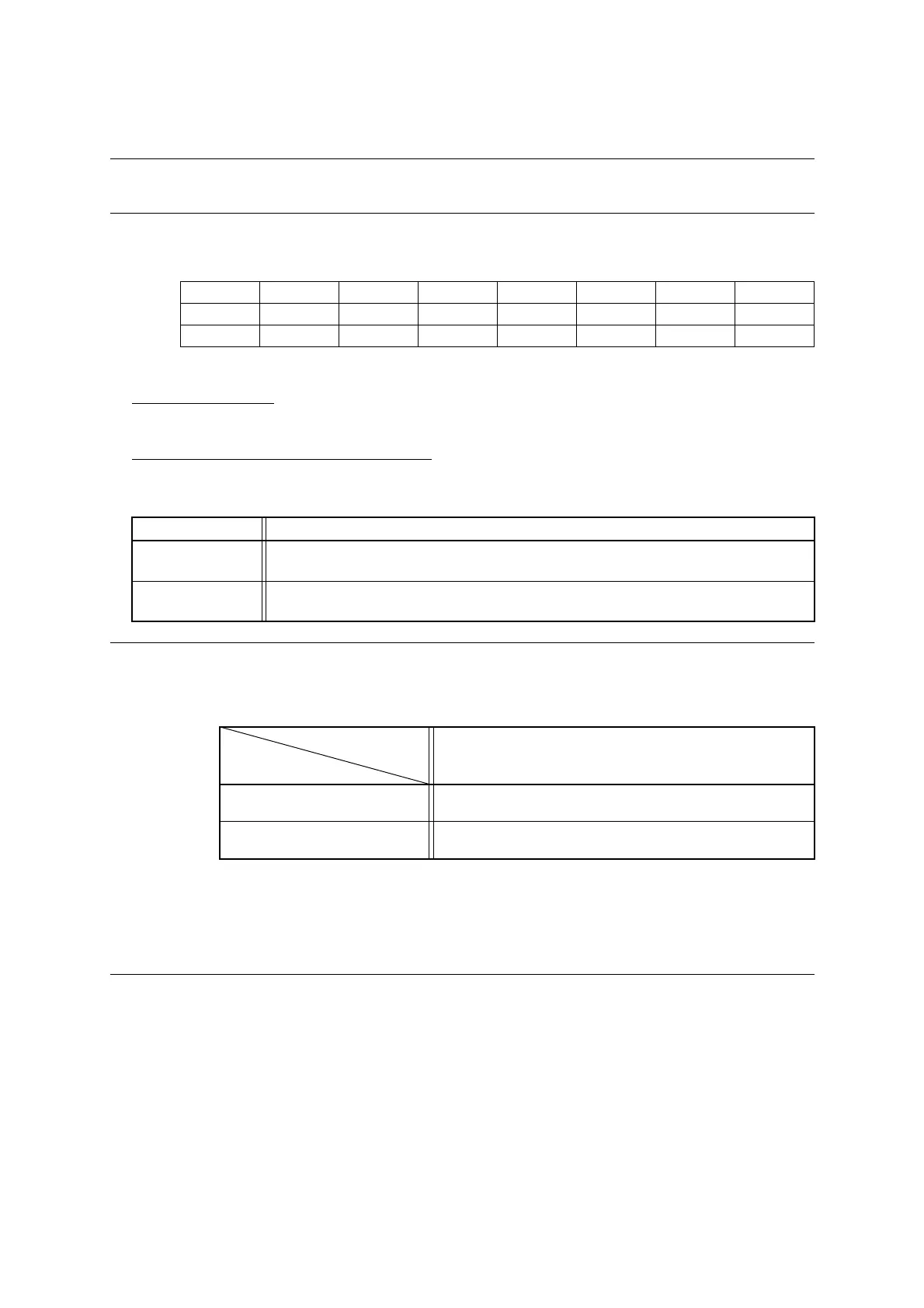
■ Register Configuration
■ Register Functions
[bit7:1] Undefined bits
Their read values are always "0". Writing values to these bits has no effect on operation.
[bit0] DSTBYX: Deep standby mode control bit
This bit makes the device transit to deep standby mode by setting the Flash memory to the low-power state in
standby mode.
Notes:
• Waking up the device from deep standby mode and waking up the device from the
normal standby mode have the following difference.
• Refer to "■ ELECTRICAL CHARACTERISTICS" in the device data sheet for the
difference between the deep standby mode and the normal standby mode in power
consumption.
• Do not make the device transit to deep standby mode when a Flash command
sequence (except read/reset) has been invoked.
bit 7 6 5 4 3 2 1 0
Field — — — — — — — DSTBYX
Attribute — — — — — — — R/W
Initial value 0 0 0 0 0 0 0 0
bit0 Details
Writing "0"
Sets the Flash memory to the low-power state when the device enters standby mode according to
the setting of the standby control register (STBC). (deep standby mode)
Writing "1"
Keeps the Flash memory at the normal state when the device enters standby mode according to
the setting of the standby control register (STBC). (normal standby mode)
Maximum time required to wake up the device from deep
standby mode
(SCLK: source clock, MCLK: machine clock)
In main clock mode, main CR clock
mode, or main CR PLL clock mode
(10 SCLK + 150 µs + 6 MCLK) +
time required to wake up the
device from normal standby mode
In subclock mode or sub-CR clock
mode
(2 SCLK + 150 µs + 6 MCLK) +
time required to wake up the
device from normal standby mode