MB95630H Series
526 FUJITSU SEMICONDUCTOR LIMITED MN702-00009-2v0-E
CHAPTER 24 I
2
C BUS INTERFACE
24.7 Registers
24.7.6 I
2
C Clock Control Register ch. n (ICCRn)
The I
2
C clock control register ch. n (ICCRn) register enables the I
2
C operation
and selects the shift clock frequency.
■ Register Configuration
■ Register Functions
[bit7] DMBP: Divider m bypass bit
This bit is used to bypass the divider m to generate the shift clock frequency.
Writing "0" to this bit sets the value set in the CS[4:3] bits as the divider m value (m = ICCRn:CS[4:3]).
When "1" is written to this bit, the divider m is to be bypassed.
Do not write "1" to this bit when the value of divider n is "4" (ICCRn:CS[2:0] = 0b000).
[bit6] Undefined bit
The read value of this bit is always "0". Writing a value to this bit has no effect on operation.
[bit5] EN: I
2
C bus interface operation enable bit
This bit enables the I
2
C bus interface operation.
Writing "0" to this bit disables the I
2
C bus interface operation and clears the following bits to "0".
• AACKX, INTS, and WUE bits in the IBCR0n register
• All bits in the IBCR1n register except the BER and BEIE bits
• All bits in the IBSRn register
Writing "1" to this bit enables the I
2
C bus interface operation.
If one of the following conditions is satisfied, this bit is set to "0".
• "0" is written to this bit.
• The BER bit in the IBCR1n register is set to "1".
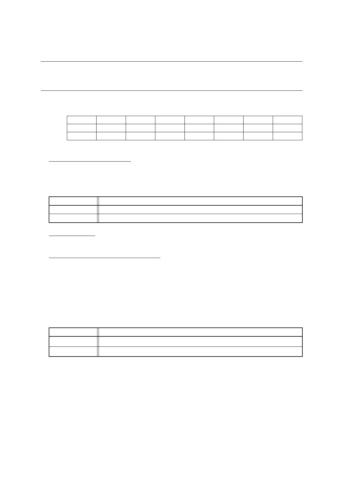
bit 7 6 5 4 3 2 1 0
Field DMBP — EN CS4 CS3 CS2 CS1 CS0
Attribute R/W — R/W R/W R/W R/W R/W R/W
Initial value 0 0 0 0 0 0 0 0
bit7 Details
Writing "0" The settings of ICCRn:CS[4:3] (clock divide m) are valid.
Writing "1" The settings of ICCRn:CS[4:3] (clock divide m) are invalid.
bit5 Details
Writing "0"
Disables the I
2
C bus interface operation.
Writing "1"
Enables the I
2
C bus interface operation.