MB95630H Series
MN702-00009-2v0-E FUJITSU SEMICONDUCTOR LIMITED 393
CHAPTER 21 MULTI-PULSE GENERATOR
21.5 Operations
■ 16-bit MPG Output Data Register (Upper/Lower) (OPDUR/OPDLR)
The content of the 16-bit MPG output data register (upper/lower) (OPDUR/OPDLR) is sent
from the 16-bit MPG output data buffer register (upper/lower) (OPDBRHB and OPDBRLB -
OPDBRH0 and OPDBRL0) according to the write timing signal (WTO) generated by the data
write control unit, and the OPTx output waveform is updated. Moreover, the output level can
be compulsorily fixed by the DTTI pin input.
The OPTx output waveform timing diagram is shown in Figure 21.5-2 and the operation is
explained in following sections.
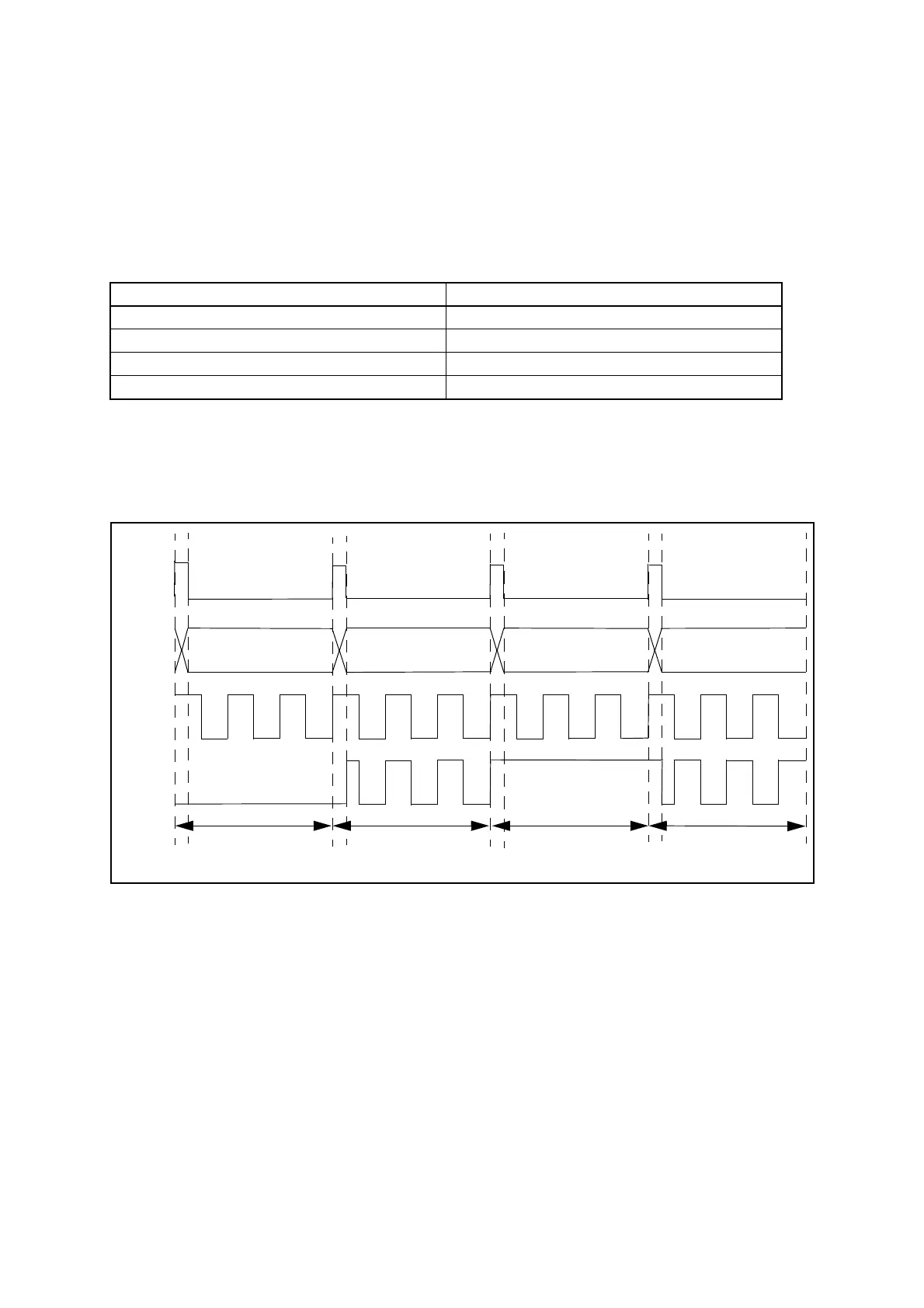
■ OPTx Output Waveform Timing Diagram (WTS[1:0] = 0b00)
Figure 21.5-2 OPTx Output Waveform Timing Diagram (WTS[1:0] = 0b00)
Table 21.5-1 16-bit MPG Output Data Register (Upper/Lower) (OPDUR/OPDLR)
OPx1,OPx0 Setting OPTx Output
OPx1,OPx0 = 0,0 "L" level
OPx1,OPx0 = 0,1 16-bit PPG timer output
OPx1,OPx0 = 1,0 16-bit PPG timer inverted output
OPx1,OPx0 = 1,1 "H" level
0b00
0b01 0b11 0b10
OPx1,
OPx0
PPG
OPTx
"L" Output
PPG Output
PPG Inverted Output
"H" Output
WTO
(OPDUR,
OPDLR)