MB95630H Series
570 FUJITSU SEMICONDUCTOR LIMITED MN702-00009-2v0-E
CHAPTER 26 DUAL OPERATION FLASH MEMORY
26.8 Registers
Settings of SAxE (x = 0, 1 or 2) and their respective programming functions:
• Program-disabled (SAxE = 0):
With "0" not written to the SAxE bit in the flash memory sector write control register 0 (SWRE0),
programming data to a sector can be enabled by setting the SAxE bit corresponding to that sector to "1".
(This is the state after a reset).
• Program-enabled (SAxE = 1):
Data can be written to a sector corresponding to the SAxE bit.
• Spurious programming prevention (SAxE = 0)
With "0" written to the SAxE bit in the flash memory sector write control register 0 (SWRE0),
programming data to a sector cannot be enabled even though the SAxE bit corresponding to that sector is
set to "1".
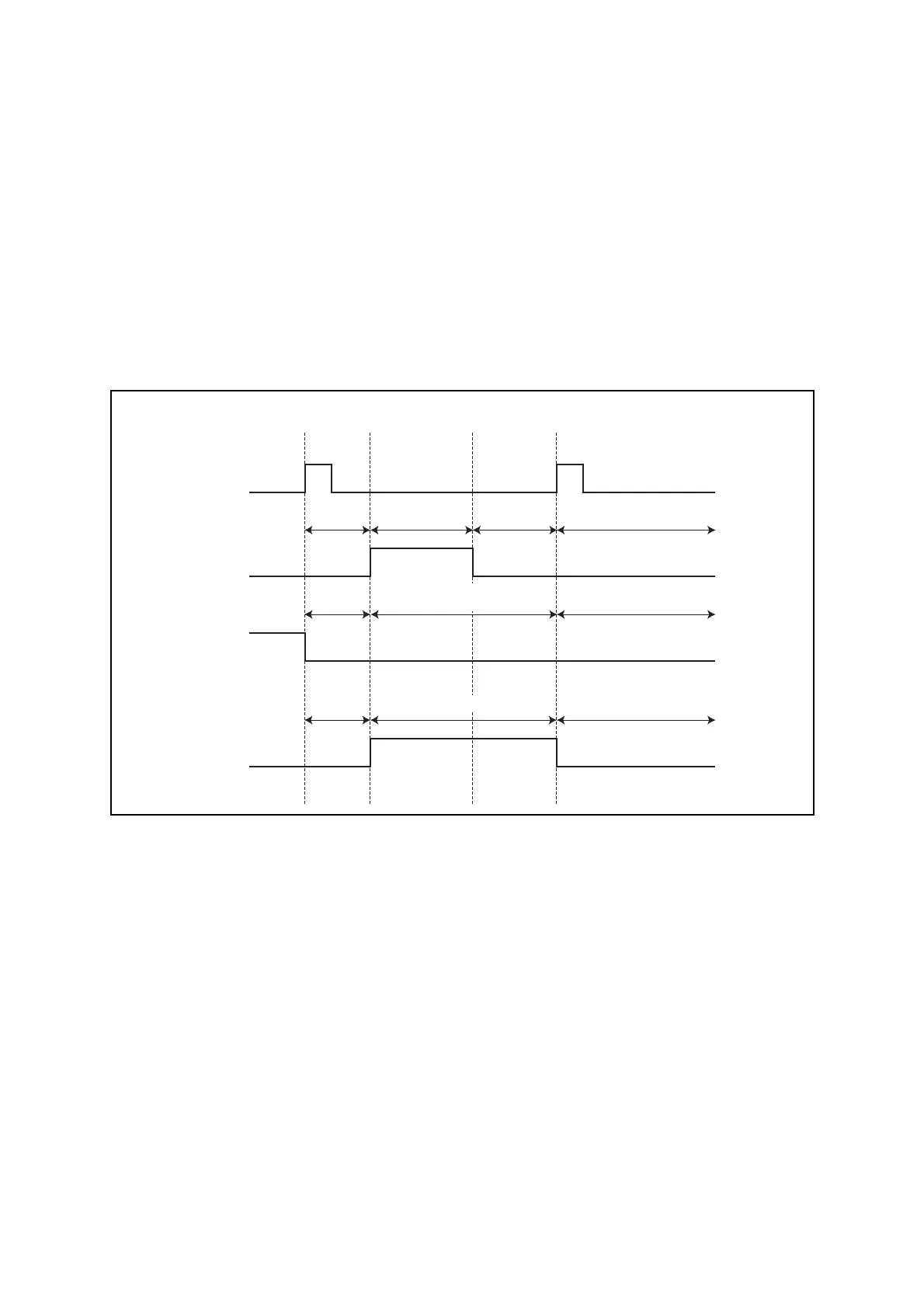
Figure 26.8-2 Examples of Flash Memory Program-disabled, Program-enabled, and Spurious
Programming Prevention States Depending on Flash Memory Sector Write Control Register 0
(SWRE0)
■ Note on Setting SWRE0 Register
To program data to or erase data from SA0 (0x1000
to 0x17FF) or SA1 (0x1800
to 0x1FFF) of
the Flash memory when FSR:SSEN is "0", set both SA0E and SA1E in the SWRE0 register to
"1" first.
To program data to or erase data when FSR:SSEN is "1", set SA0E, SA1E and SA2E in the
SWRE0 register to "1" first.
For details of the sector map of the Flash memory, see Figure 26.2-1 and Figure 26.8-1.
Program-enabled Program-disabled
Program-disabled
Program-disabled
RST
SA0E
SA1E
SA2E
Initialize Initialize
Write access
to register
Write access
to register
Program-enabled
Program-
disabled
Program-
disabled
Program-
disabled
Spurious programming
prevention
Spurious
programming
prevention