MB95630H Series
MN702-00009-2v0-E FUJITSU SEMICONDUCTOR LIMITED 395
CHAPTER 21 MULTI-PULSE GENERATOR
21.5 Operations
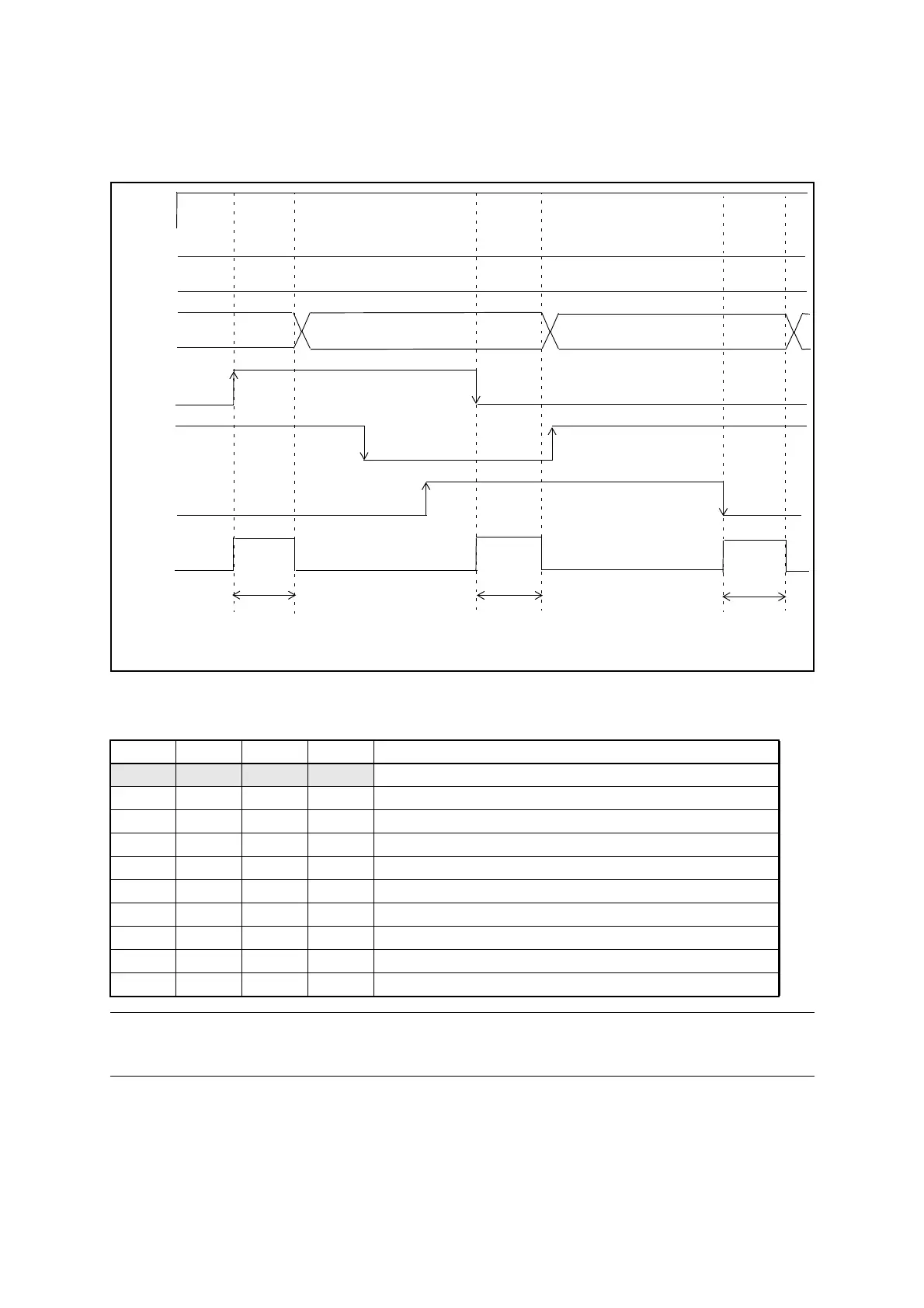
■ Both Edges Detection and SNIx/RDAx Comparison Timing Diagram
(CMPE = 1)
Figure 21.5-4 Both Edges Detection and SNIx/RDAx Comparison Timing Diagram (CMPE = 1)
■ WTIN1 Output Condition and Register Setting
Note:
When CMPE = 1, SEEx should be set to "0", setting SEEx = 1 is not recommended.
Table 21.5-2 WTIN1 Output Condition and Register Setting
CMPE CPE1 CPE0 SEEx WTIN1 Output Condition
0 0 0 0 No output. (Initial value)
0 0/1 0/1 0 No output.
0 0 0 1 No output.
0 0 1 1 Detects SNIx rising edge.
0 1 0 1 Detects SNIx falling edge.
0 1 1 1 Detects SNIx both edges.
1 0 0 0/1 Setting prohibited.
1 0 1 0/1 Detects SNIx rising edge and SNIx/RDAx comparison match.
1 1 0 0/1 Detects SNIx falling edge and SNIx/RDAx comparison match.
1 1 1 0/1 Detects SNIx both edges and SNIx/RDAx comparison match.
0b0010b110
0b010
WTIN1
RDA[2:0]
(OPDUR)
SNI0
SNI1
SNI2
CMPE
COMPARISON
MATCH
COMPARISON
MATCH
COMPARISON
MATCH
0b11
CPE1,
CPE0