MB95630H Series
418 FUJITSU SEMICONDUCTOR LIMITED MN702-00009-2v0-E
CHAPTER 21 MULTI-PULSE GENERATOR
21.5 Operations
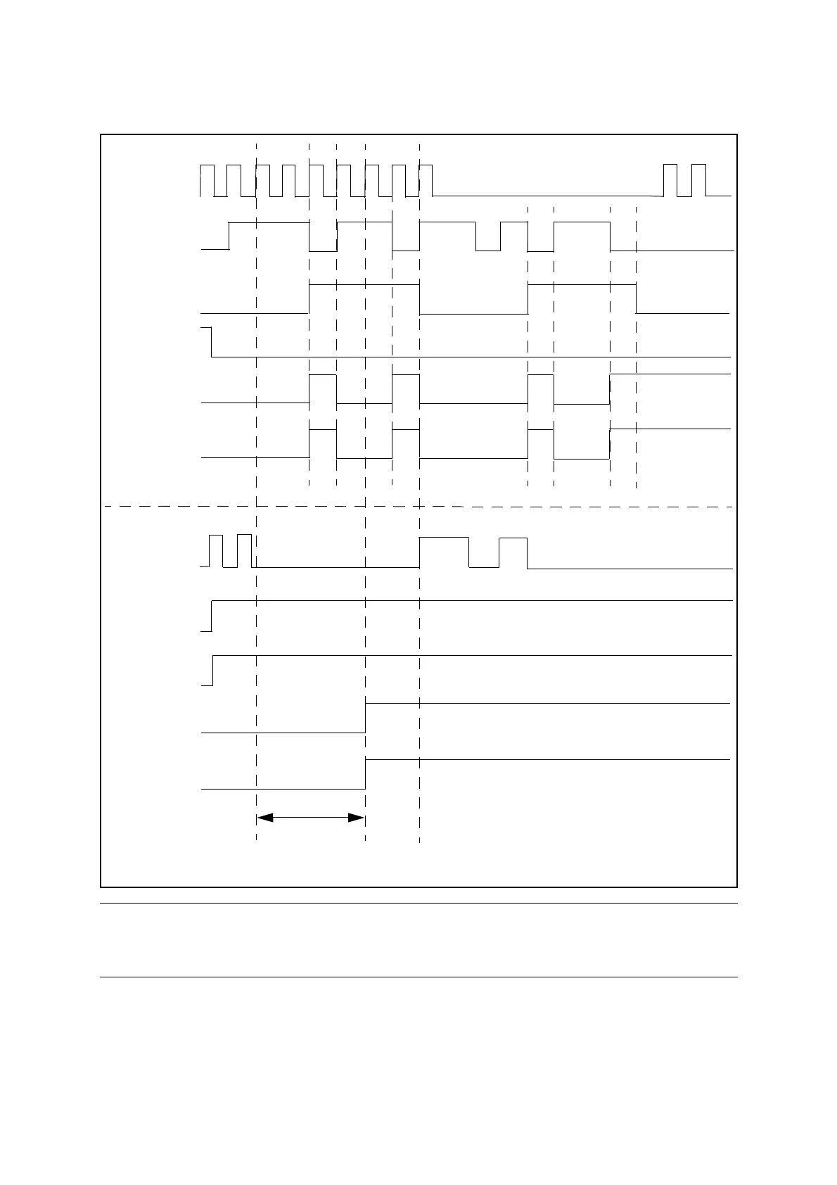
■ DTTI Circuit Timing Diagram (D[1:0] = 0b00)
Figure 21.5-26 DTTI Circuit Timing Diagram (D[1:0] = 0b00)
Note:
In the worst case the time from DTTI being recognized (after noise cancellation) to DTISP
in effect takes 2 cycles, in best case it takes 1 cycle.
DTTI
DTIF*
DTIE
DTTI
DTIF*
NRSL
NRSL
DTIE
DTISP
DTISP
4 Cycles
MCLK
* DTIF is cleared by writing “0” to it.