GEN7iB
156
INTERFACE/CONTROLLER
INTERFACE/CONTROLLER
11
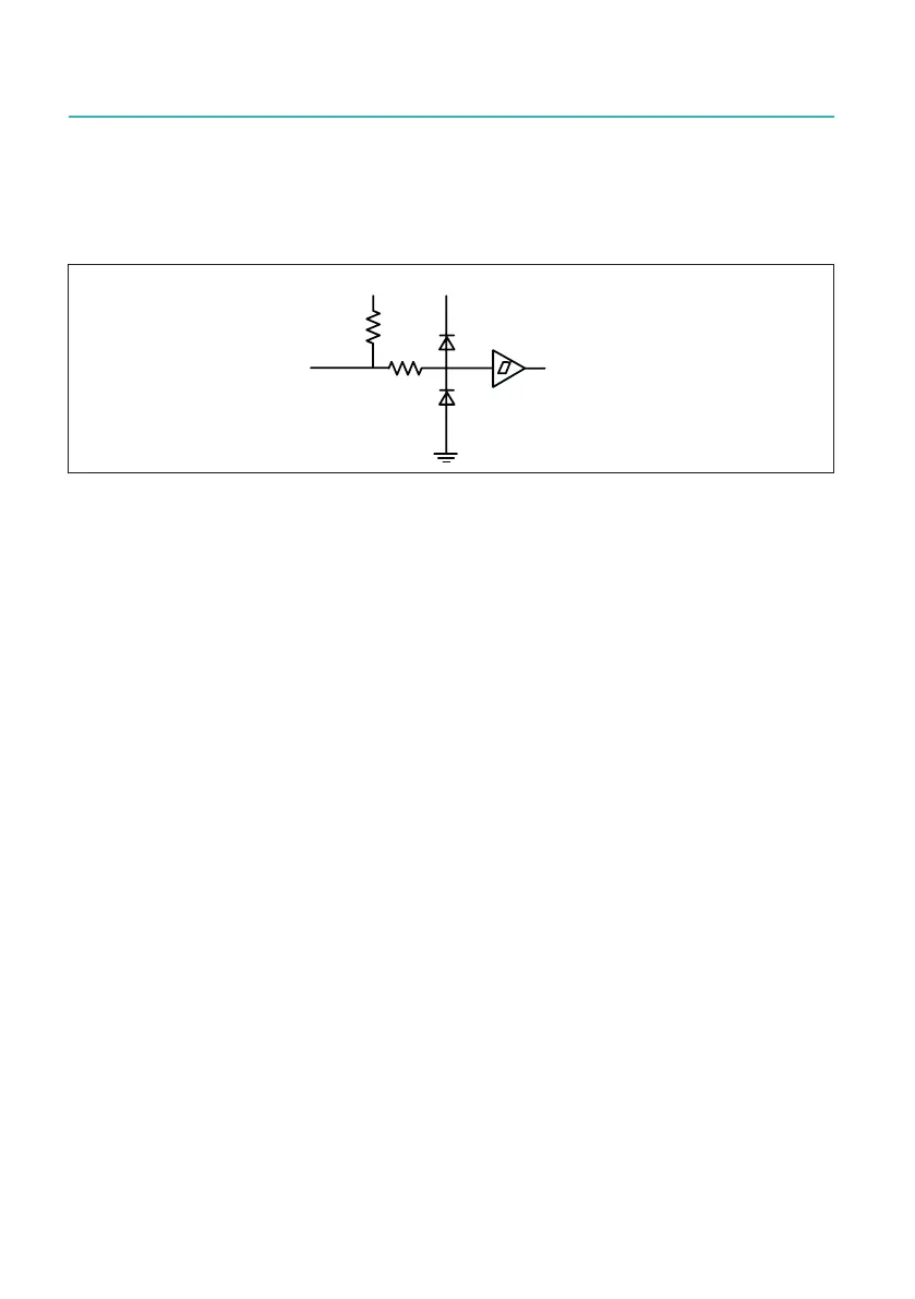
11.4.1 I/O connector input overvoltage protection
All inputs of the I/O connector are over voltage protected. All inputs use the following
schematic approach.
7RV\VWHPWLPEDVHWULJJHU
DQGUHFRUGLQJFRQWURO
U
N2KP
N2KP
Fig. 11.11 I/O connector schematic inputs
Duetothe20kΩpull-upresistorallinputswillbe“TTLHigh”andonlyneedanexternal
shorttosignalgroundtobeoperated.The2kΩseriesresistortogetherwiththediode
clampstogroundand+5Vprotectthedigitalcircuitryuptothespeciedvoltages.
The clamping diodes and other parasitic capacitors do create a capacitive load on
your signal source and limit the signal bandwidth. To reach the required bandwidths
detailed compensations are made not addressed in this block diagram.
 Loading...