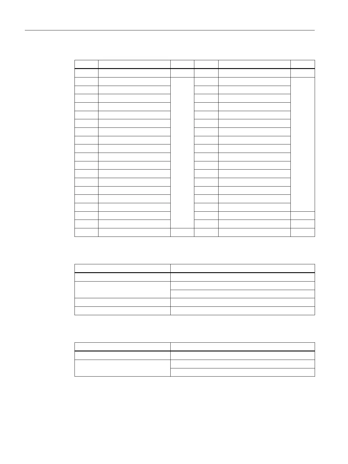
Table 7-53 Assignment of connector X114
Pin Signal name Type Pin Signal name Type
1 Ground V 2 Ground V
3 DI118.0 I 4 DO118.0 O
5 DI118.1 6 DO118.1
7 DI118.2 8 DO118.2
9 DI118.3 10 DO118.3
11 DI118.4 12 DO118.4
13 DI118.5 14 DO118.5
15 DI118.6 16 DO118.6
17 DI118.7 18 DO118.7
19 DI119.0 20 DO119.0
21 DI119.1 22 DO119.1
23 DI119.2 24 DO119.2
25 DI119.3 26 DO119.3
27 DI119.4 28 DO119.4
29 DI119.5 30 DO119.5
31 DI119.6 32 DO119.6
33 DI119.7 34 DO119.7
35 DI121.4 36 DI121.5 I
37 DI121.6 38 DI121.7 I
39 Reserved 40 Reserved
Table 7-54 Technical data of the inputs of X111 to X114
Parameter Value
Voltage: 0 V to 5 V
Typical current consumption: 0.2 mA at 5 VDC
-0.3 mA at 0 VDC
Signal level (including ripple): High signal level: 2.3 V to 5 V
Low signal level: 0 V to 1 V
Table 7-55 Technical data of the outputs of X111 to X114
Parameter Value
Voltage: 0 V to 5 V (depending on the load)
Typical load current (without external
series resistor):
8 mA at LED flow voltage = 2.3 V
15 mA at short-circuit
Anschließbare Komponenten
7.5 MCP Interface PN
PPU and components
168 Manual, 05/2015, 6FC5397-2DP40-3BA4
 Loading...