Coding Interrupts
Grouped ISR (Interrupt Service Routine)
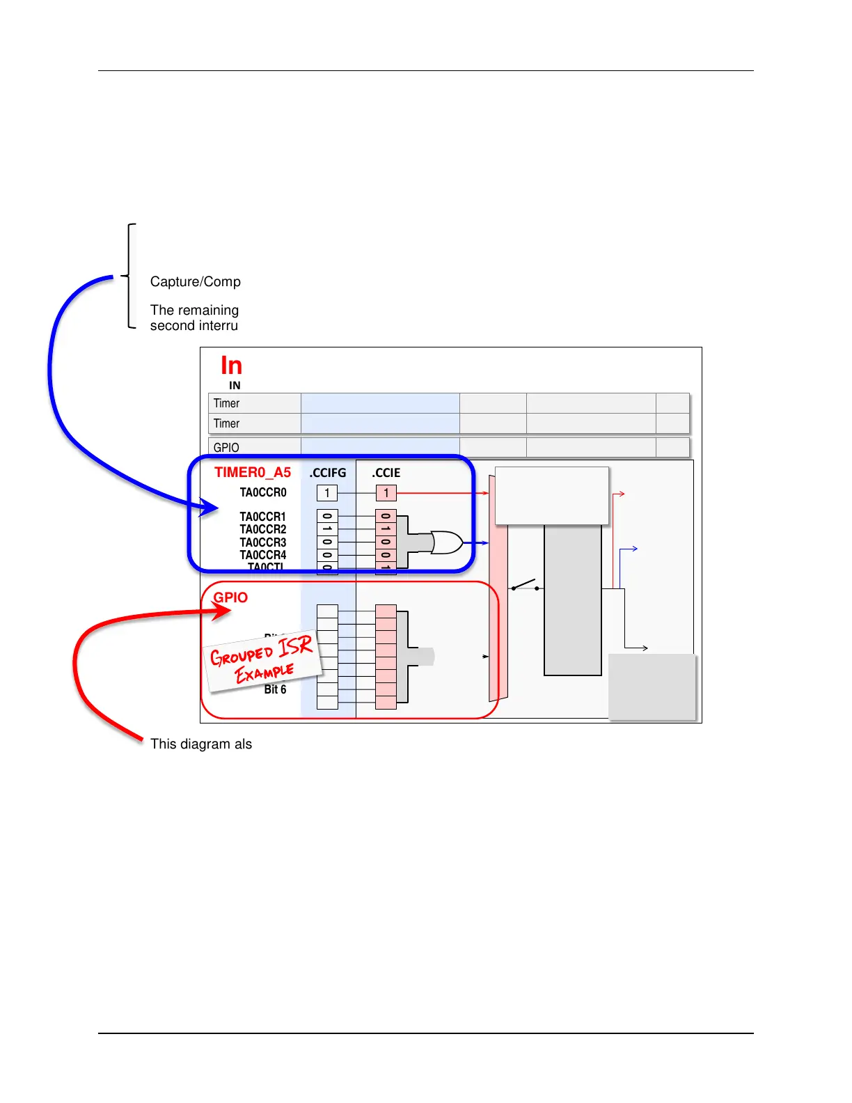
Logical Diagram for Grouped Interrupts
Before examining the code for a grouped ISR, let’s first examine the grouped interrupt using a
logical diagram.
As we briefly mentioned earlier in the chapter (and will discuss in full detail in a later chapter), the
Timer_A and Timer_B peripherals are provided with two interrupts. For example, when looking at
Timer0_A5, there is a dedicated interrupt for TA0CCR0 (which stands for Timer0_A
Capture/Compare Register 0). Notice below how this is routed directly to the GIE input mux.
The remaining five Timer0_A5 interrupts are logically AND’d together; this combination provides a
second interrupt signal from Timer0_A5 to the GIE input mux.
Individual & Multiple Interrupt Sources
CPU
0 1 0
0
0
)
0 1 0 0 1
TIMER0_A5
TA0CCR1
TA0CCR2
TA0CCR3
TA0CCR4
TA0CTL
.CCIFG .CCIE
1 1
TA0CCR0
0
1 0
0
0 1 1 1
0 1 0 0 1 1 0 0
)
GPIO Port 1
P1IFG P1IE
Bit 0
Bit 1
Bit 2
Bit 3
Bit 4
Bit 5
Bit 6
Bit 7
SR.GIE
52
TA0IV
53
INT Source IFG
47
47
Example:
Interrupts on
pin 1 and 5
Reading P1IV
returns highest
priority interrupt
and clears it’s
IFG bit
Single interrupt:
Only caused by one
INT – simplifies ISR
IFG auto cleared
This diagram also shows that all of the input pins for GPIO port 1 (P1) share a single, grouped
interrupt. This means your GPIO ISR must always verify which pin actually caused an interrupt
whenever the ISR is executed.
The interrupt logic within the CPU recognizes each of these interrupt sources, therefore:
• If the first interrupt (TA0CCR0) occurs, it will cause the code at vector address 53
(TIMER_A0_VECTOR) to be executed.
• Similarly, the remaining Timer0 interrupts are associated with vector 52.
• Finally, the GPIO port (P1) was assigned (by the chip designer) to vector 47.
5 - 24 MSP430 Workshop - Interrupts