Miscellaneous Topics
GPIO Interrupt Summary
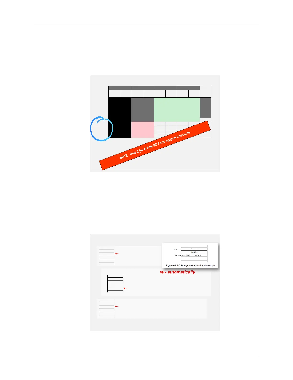
The diagram used to summarize the GPIO control registers in a previous chapter is a good way
to visualize the GPIO interrupt capabilities of our devices. From the diagram below we can see
that most MSP430 processors allow ports P1 and P2 to be used as external interrupt sources; we
see this from the fact that these ports actually have the required port interrupt registers.
GPIO Interrupt Register Summary
PA PB PC PD
PJ*
(4-bit )
P1
†
P2 P3 P4 P5 P6 P7
P8
(3-bit)
PxIN
All
Three
Devices
support
F5529
and
FR5969
(only)
F5529
(only)
F55
&
FR59
PxDS
PxSEL
PxIV
FR5969 (only)
PxIES
PxIE
PxIFG
P1IV: Interrupt Vector generator
Highest Priority Pending interrupt enabled on Port 1
P1IES: Interrupt Edge Select
Are interrupts triggered on high/low edge? (0 = low-to-high)
P1IE: Interrupt Enable register for Port 1
P1IFG: Interrupt Flag register for Port 1
There are other devices in the MSP430 family that support interrupts on more than 2 ports, but of
the three example processors we use throughout this course, only the FR5969 (Wolverine)
devices support interrupt inputs on additional ports (P3 and P4).
Interrupt Processing Flow
The following information was previously covered in this chapter, but since the slide is a good
summary of the interrupt processing flow, we have included it anyway.
ISR hardware - automatically
PC pushed
SR pushed
Interrupt vector moved to PC
GIE, CPUOFF, OSCOFF and SCG1 cleared
IFG flag cleared on single source flags
reti - automatically
SR popped - original
PC popped
Prior to ISR
SP
Item1
Item2
PC
SR
SP
SP
Item1
Item2
Item1
Item2
PC
SR
Interrupt Processing
5 - 30 MSP430 Workshop - Interrupts