Figure 99. Address Configuration of Flash Memory ........................................................................... 189
Figure 100. The Sequence of Page Program and Erase of Flash Memory ........................................ 190
Figure 101. The Sequence of Bulk Erase of Flash Memory ............................................................... 191
Figure 102. ISP Mode ......................................................................................................................... 195
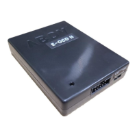
Figure 103. Using OCD/E-PGM+/E-GANG4/E-GANG6. .................................................................... 200
Figure 104. AC Timing ......................................................................................................................... 207
Figure 105. SPI master mode timing (UCPHA = 0, MSB first) ............................................................ 209
Figure 106. SPI/Synchronous master mode timing (UCPHA = 1, MSB first)...................................... 209
Figure 107. SPI slave mode timing (UCPHA = 0, MSB first) .............................................................. 210
Figure 108. SPI/Synchronous slave mode timing (UCPHA = 1, MSB first) ........................................ 210
Figure 109. SPI0/1 Timing................................................................................................................... 211
Figure 110. I2C Timing ........................................................................................................................ 212
Figure 111. Stop Mode Release Timing when Initiated by an Interrupt .............................................. 213
Figure 112. Stop Mode Release Timing when Initiated by RESETB .................................................. 213
Figure 113. Crystal/Ceramic Oscillator ............................................................................................... 215
Figure 114. External Clock .................................................................................................................. 215
Figure 115. Crystal Oscillator .............................................................................................................. 216
Figure 116. Crystal Oscillator .............................................................................................................. 216
Figure 117. Clock Timing Measurement at XIN .................................................................................. 217
Figure 118. Clock Timing Measurement at SXIN ................................................................................ 217
Figure 119. Operating Voltage Range ................................................................................................. 218
Figure 120. Recommended Voltage Range ........................................................................................ 218
Figure 121. RUN (IDD1) Current ........................................................................................................ 219
Figure 122. IDLE (IDD2) Current ........................................................................................................ 220
Figure 123. SUB RUN (IDD3) Current ................................................................................................ 220
Figure 124. SUB IDLE (IDD4) Current ................................................................................................ 221
Figure 125. SUB IDLE (IDD4) Current ................................................................................................ 221
Figure 126 16 SOPN Package Outline ............................................................................................... 222
Figure 127. 20 TSSOP Package Outline ............................................................................................ 223
Figure 128. 20 SOP Package Outline ................................................................................................. 224
Figure 129. 24 QFN Package Outline ................................................................................................. 225
Figure 130. 28 SOP Package Outline ................................................................................................. 226
Figure 131. 32 LQFP Package Outline ............................................................................................... 227
Figure 132. Debugger (OCD1/OCD2) and Pinouts ............................................................................ 228
Figure 133. E-PGM+ (Single Writer) and Pinouts ............................................................................... 229
Figure 134. E-Gang4 and E-Gang6 (for Mass Production) ................................................................ 230
Figure 135. PCB Design Guide for On-Board Programming .............................................................. 231
Figure 136. On-Chip Debugging System in Block Diagram ................................................................ 232
Figure 137. 10-bit Transmission Packet .............................................................................................. 233
Figure 138. Data Transfer on Twin Bus .............................................................................................. 234
Figure 139. Bit Transfer on Serial Bus ................................................................................................ 234
Figure 140. Start and Stop Condition .................................................................................................. 234
Figure 141. Acknowledge on Serial Bus ............................................................................................. 235
Figure 142. Clock Synchronization during Wait Procedure ................................................................ 235
Figure 143. Connection of Transmission ............................................................................................ 236
Figure 144. A96G166/A96A166/A96S166 Device Numbering Nomenclature .................................... 238