5.8 Measuring Optical Amplifier (Wavelength Division Multiplex)
5-75
5
Table 5.8.3-1 Setting Range of the Parameters in the Opt Amp Test Parameter
Dialog Box
Item Min. Max. Unit
1
1
2
*1: The Fitting Span is set with Signal Wl as a center. The noise location
of Fitting Span and Masked Span is Signal Wl ± Fitting Span/2. Note
that the calculation method is different from that of Point.
*2: Point is the location using Signal Wl as a reference. The noise
location is Signal Wl ± Point. Note that the calculation method is
different from that of Fitting Span and Masked Span.
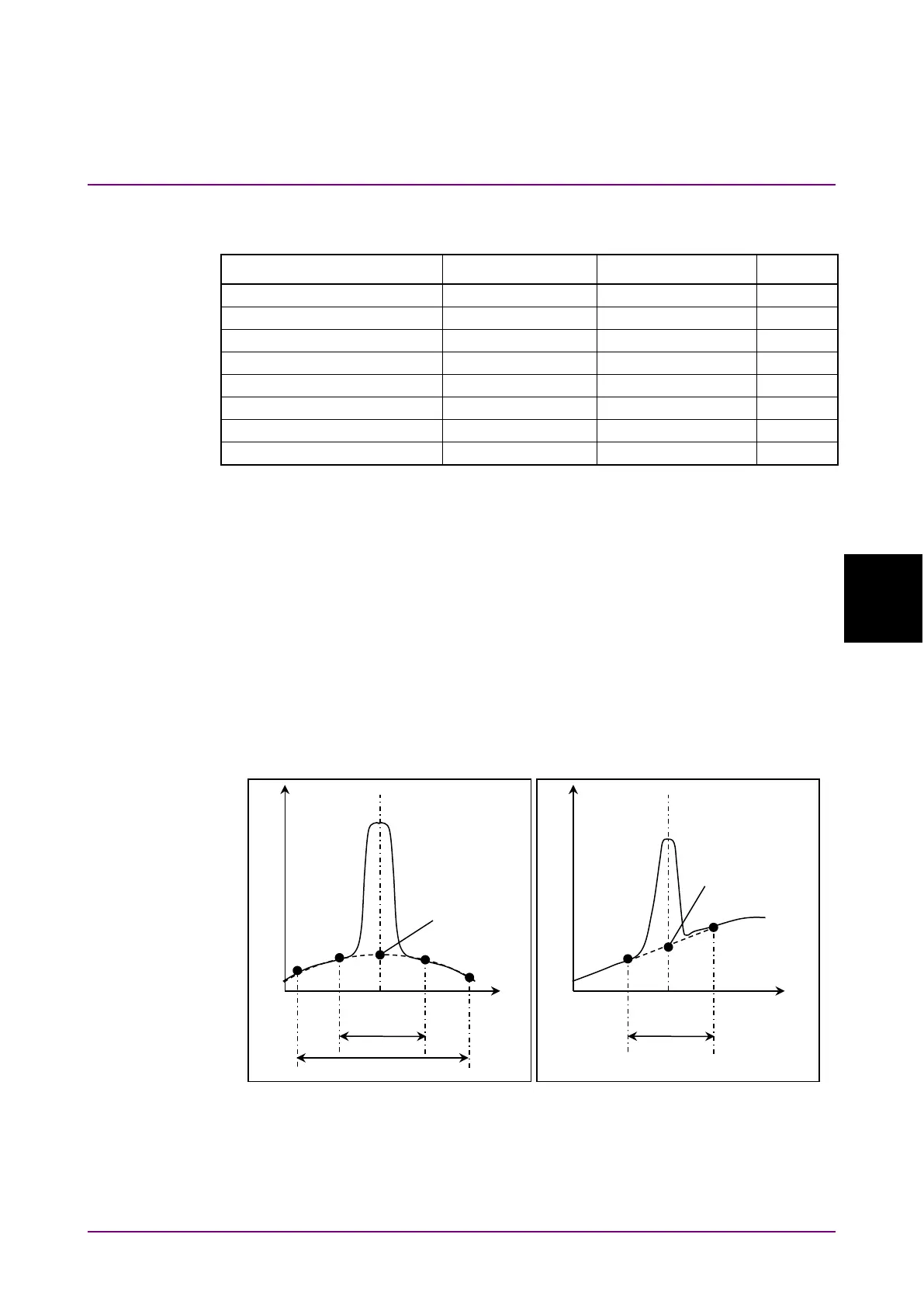
●
Detection Type
Area: The noise level is estimated from the value of fitting curve at
signal wavelength. The fitting curve is calculated from the
noise wavelength in the Area
Point: The noise level is estimated by linear interpolation from the
position set for the Point.
Figure 5.8.3-2 Detection Method for Estimated Noise Level
Wavelength (nm)
Level
Estimate
noise level
Masked Span
Wavelength (nm)
Level
Estimate
noise level
Point