5-1
Chapter 5. Functions
5 - 1 PV Input
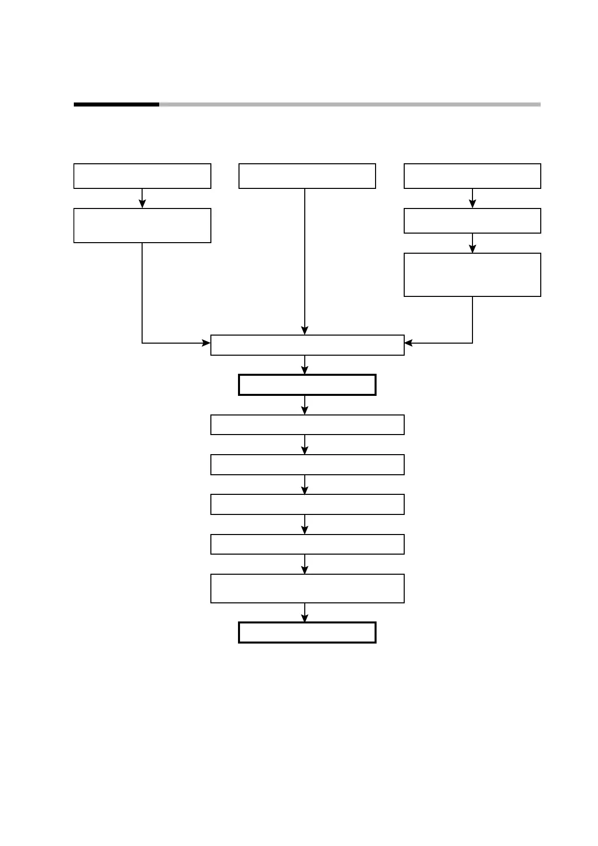
The following is a functional block diagram for PV input.
For thermocouple For RTD For DC voltage/current
PV input range type
(Setup bank: C01)
PV input range type
(Setup bank: C01)
PV input range type
(Setup bank: C01)
Reference junction compensation
(cold junction compensation)
(Setup bank: C03)
PV square root extraction dropout
(Setup bank: C09)
(Setup bank: C04 to C06)
PV low and high limit alarm
PV before applying ratio, bias, lter
PV ratio (Parameter bank: rA)
PV bias (Parameter bank: bI)
PV lter (Parameter bank: FL)
PV low/high limits
PV hold
(DI assignment bank: operation type: dI1.1 to 3.1)
PV
Decimal point position,
PV range low limit,
PV range high limit