MB95630H Series
172 FUJITSU SEMICONDUCTOR LIMITED MN702-00009-2v0-E
CHAPTER 11 8/16-BIT COMPOSITE TIMER
11.14 Registers
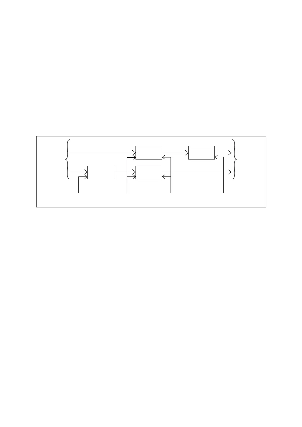
● Read and write operations
Read and write operations of Tn0DR and Tn1DR are performed in the following manner in 16-
bit operation or when the PWM timer function (variable-cycle) is selected.
• Read from Tn1DR: In addition to the read access to Tn1DR, the value of Tn0DR is
also stored in the internal read buffer at the same time.
• Read from Tn0DR: The internal read buffer is read.
• Write to Tn1DR: Data is written to the internal write buffer.
• Write to Tn0DR: In addition to the write access to Tn0DR, the value of the internal
write buffer is stored in Tn1DR at the same time.
Figure 11.14-1 shows the Tn0DR and Tn1DR registers read from and written to during 16-bit
operation.
Figure 11.14-1 Read and Write Operations of Tn0DR and Tn1DR Registers during 16-bit
Operation
Tn0DR
register
Tn1DR
register
Read
buffer
Write
buffer
Tn1DR
write
Tn0DR
write
Tn1DR
read
Tn0DR
read
Read
data
Write
data