MB95630H Series
256 FUJITSU SEMICONDUCTOR LIMITED MN702-00009-2v0-E
CHAPTER 14 LIN-UART
14.7 Registers
[bit4] SCDE: Serial clock delay enable bit
In operating mode 2 in which the serial clock transmission side is selected, if the SCDE bit is set to "1", a
delayed serial clock as shown in Figure 14.6-5 is output. The function of outputting delayed serial clock can
be used in the Serial Peripheral Interface (SPI).
This bit is fixed at "0" in operating mode 0/1/3.
[bit3] SSM: Start/stop bits mode enable bit
In operating mode 2, if this bit is set to "1", the start/stop bits are added to the synchronous data format.
In operating mode 0/1/3, this bit is fixed at "0".
[bit2] Reserved bit
Always set this bit to "0".
[bit1] RBI: Receive bus idle detection flag bit
If the SIN pin is at "H" level and no reception is executed, this bit is "1". Do not use this bit when SSM = 0 in
operating mode 2.
[bit0] TBI: Transmit bus idle detection flag bit
If there is no transmission on the SOT pin, this bit is "1". Do not use this bit when SSM = 0 in operating
mode 2.
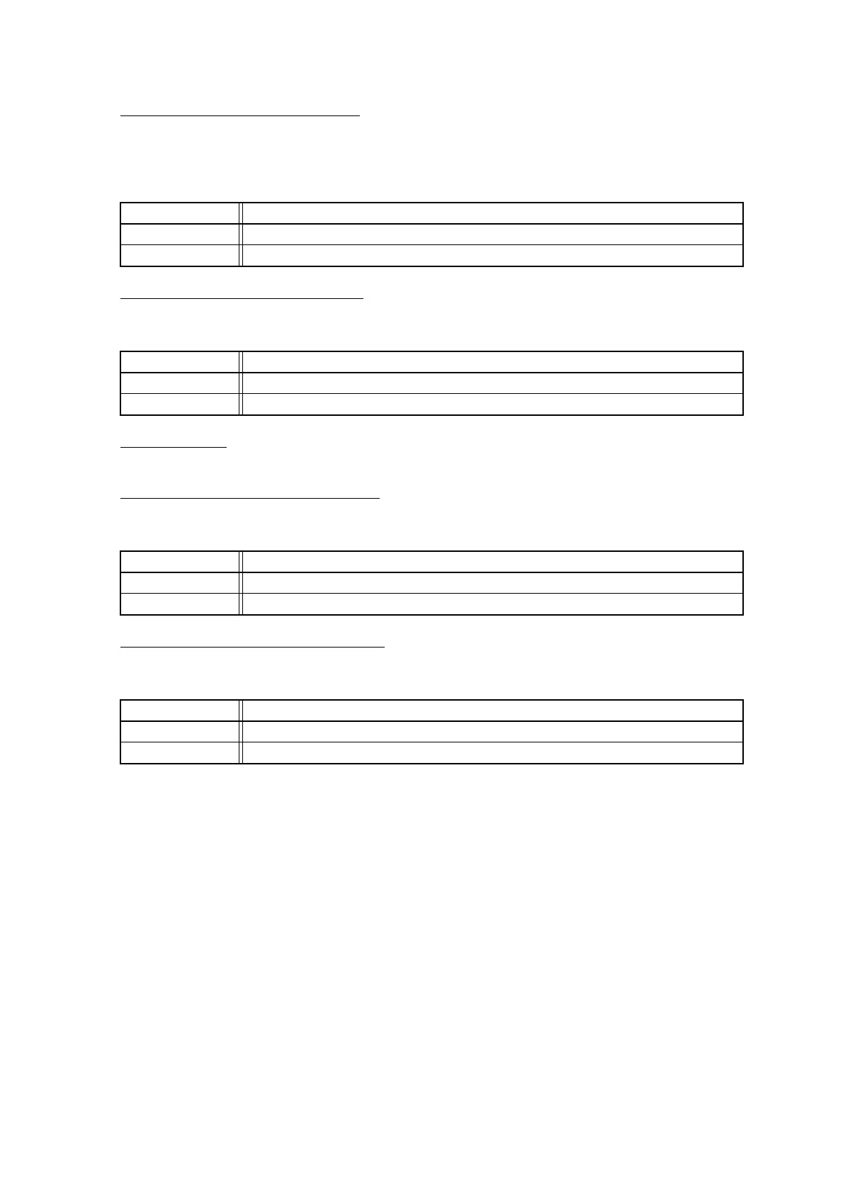
bit4 Details (only for operating mode 2)
Writing "0" Disables serial clock delay.
Writing "1" Enables serial clock delay.
bit3 Details (only for operating mode 2)
Writing "0" Disables the start/stop bits.
Writing "1" Enables the start/stop bits.
bit1 Details
Reading "0" Indicates that reception is in progress.
Reading "1" Indicates that there is no reception operation.
bit0 Details
Reading "0" Indicates that transmission is in progress.
Reading "1" Indicates that there is no transmission operation.