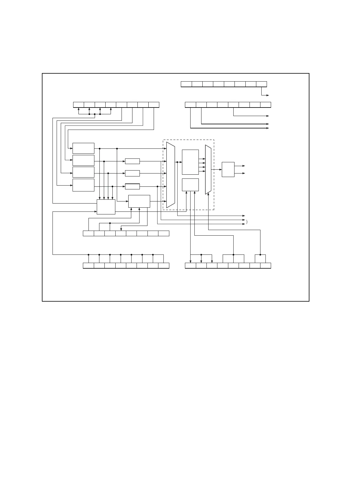
Standby control register (STBC)
System clock selector
Divide by 2
Divide by 2
Clock
control
circuit
Oscillation
stabilization
wait circuit
Supply to CPU
Supply to perip-
heral resources
Source clock
selection
control circuit
System clock control register 2 (SYCC2)
(7)
(8)
(1): Main clock (F
CH
)
(2): Subclock (F
CL
)
(3): Main clock
(4): Subclock
(5): Main CR clock (F
CRH
)
(6): Sub-CR clock (F
CRL
)
(7): Source clock (SCLK)
(8): Machine clock (MCLK)
(9): Main CR PLL clock (F
MCRPLL
)
Main CR
clock oscillator
circuit
Main clock
oscillator
circuit
Subclock
oscillator
circuit
Main CR PLL
clock oscillator
circuit
Sub-CR
clock oscillator
circuit
Divide by 2
(5)
(6)
(9)
(1)
(2)
(3)
(4)
Watch or time-base
timer mode
Sleep mode
Stop mode
Clock for time-base timer
Clock for watch timer
MPEN - - - -
MPMC1 MPMC0 MPRDY
SRDY
SOSCE MOSCE
SCRE MCREMRDY
SCRDY MCRDY
STP TMD - - -SLP SPL SRST
Standby control register 2 (STBC2)
To Flash memory
- - - -
DSTBYX
- - -
System clock control register (SYCC)
SCM2 SCS1 SCS0 DIV1 DIV0SCM1 SCM0 SCS2
Oscillation stabilization wait time setting register (WATR)
PLL control register (PLLC)
SWT3 MWT3 MWT2 MWT1 MWT0SWT2 SWT1 SWT0
Prescaler
No division
Divide by 4
Divide by 8
Divide by 16