MB95630H Series
382 FUJITSU SEMICONDUCTOR LIMITED MN702-00009-2v0-E
CHAPTER 21 MULTI-PULSE GENERATOR
21.2 Block Diagram
● 16-bit reload timer
The 16-bit reload timer is used to act as the interval timer for the waveform sequencer. Details
of the 16-bit reload timer are described in "CHAPTER 20 16-BIT RELOAD TIMER".
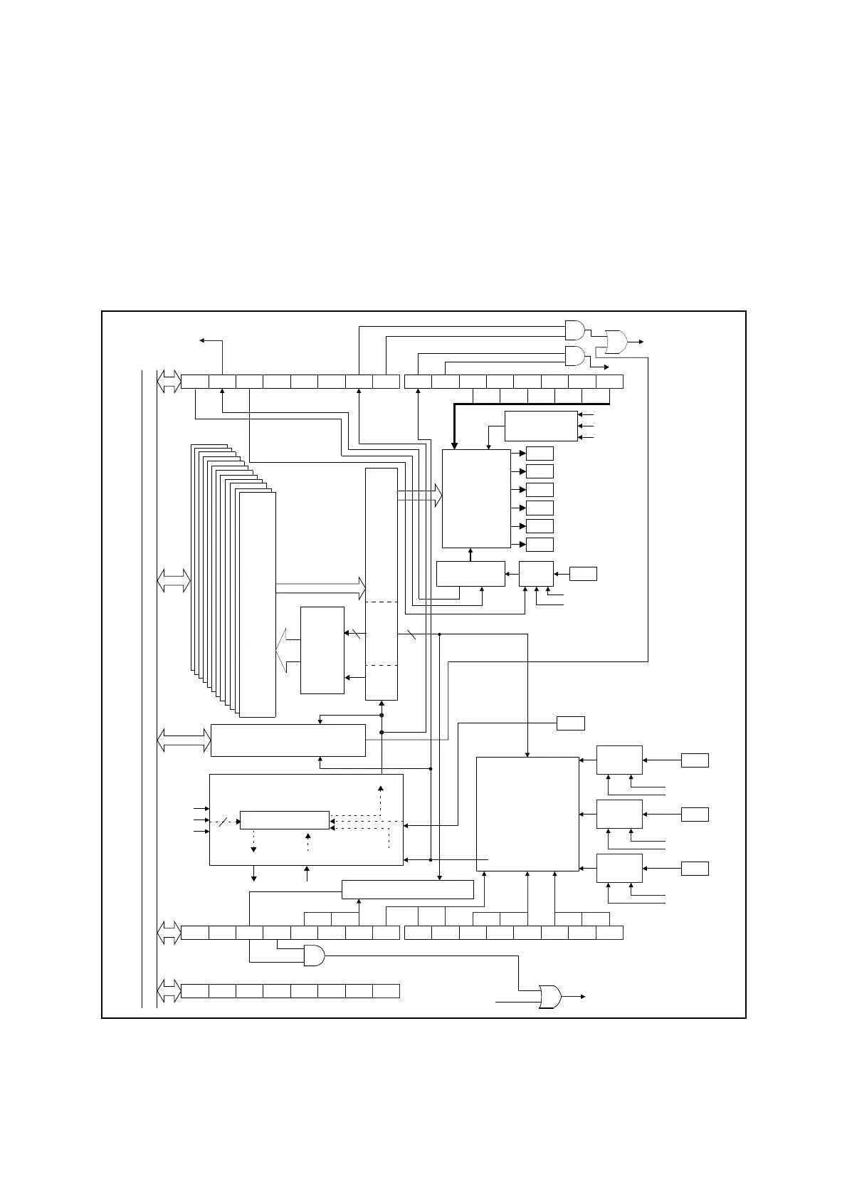
● Waveform sequencer
The waveform sequencer is the core of the multi-pulse generator, which can generate various
waveforms. Its block diagram is shown in Figure 21.2-2.
■ Block Diagram of Waveform Sequencer
Figure 21.2-2 Block Diagram of Waveform Sequencer
*: See "■ Multi-pulse Generator Interrupt Sources" in "21.4 Interrupts".
OPx1/OPx0
Decoder
F
2
MC-8FX Bus
TIN0O
WTIN0
WTIN1
WTO
RDA[2:0]
OPDBRHB and OPDBRLB to
OPDBRH0 and OPDBRL0 Registers
OPDUR Register
+
OPDLR Register
Data Write Control Unit
3
3
16-bit Timer
16-BIT MPG OUTPUT DATA BUFFER REGISTER × 12
OPDBRHx Register + OPDBRLx Register
WTIN1
BNKF
CCIRT
PPG1
WTO
TIN0O
WTIN0
3
DTTI Control
Circuit
OPCUR Register OPCLR Register
Comparison Circuit
IPCUR Register
IPCLR Register
Sync Circuit
WTS1
WTS0
Write Timing Interrupt
Compare Match Interrupt
Compare Clear Interrupt
Position Detection Interrupt
Interrupt C*
PDIRT
D1
D0
NCCR Register
Position
Detect
Circuit
Output
Control
Circuit
WTIN1
PDIRT
Interrupt A*
WTS1
WTS0 CPIF CPIE CPD2 CPD1 CPD0 CMPE
S21 S20 S11 S10 S01 S00 D1 D0
CPE1 CPE0 SNC2 SNC1 SNC0 SEE2 SEE1 SEE0
DTIE DTIF NRSL OPS2 OPS1 OPS0
WTIF
WTIE PDIF PDIE OPE5 OPE4 OPE3 OPE2 OPE1 OPE0
Pin
Pin
TI1
SNI0
Pin
SNI1
Pin
SNI2
S01
S00
Pin
DTTI
Pin
Pin
Pin
Pin
Pin
Pin
OPT0
OPT1
OPT2
OPT3
OPT4
OPT5
Noise
Filter
Interrupt B*
OPS2
Selector
OPS1
OPS0
Noise
Filter
Noise
Filter
Noise
Filter
S21
S20
S11
S10