MB95630H Series
MN702-00009-2v0-E FUJITSU SEMICONDUCTOR LIMITED 397
CHAPTER 21 MULTI-PULSE GENERATOR
21.5 Operations
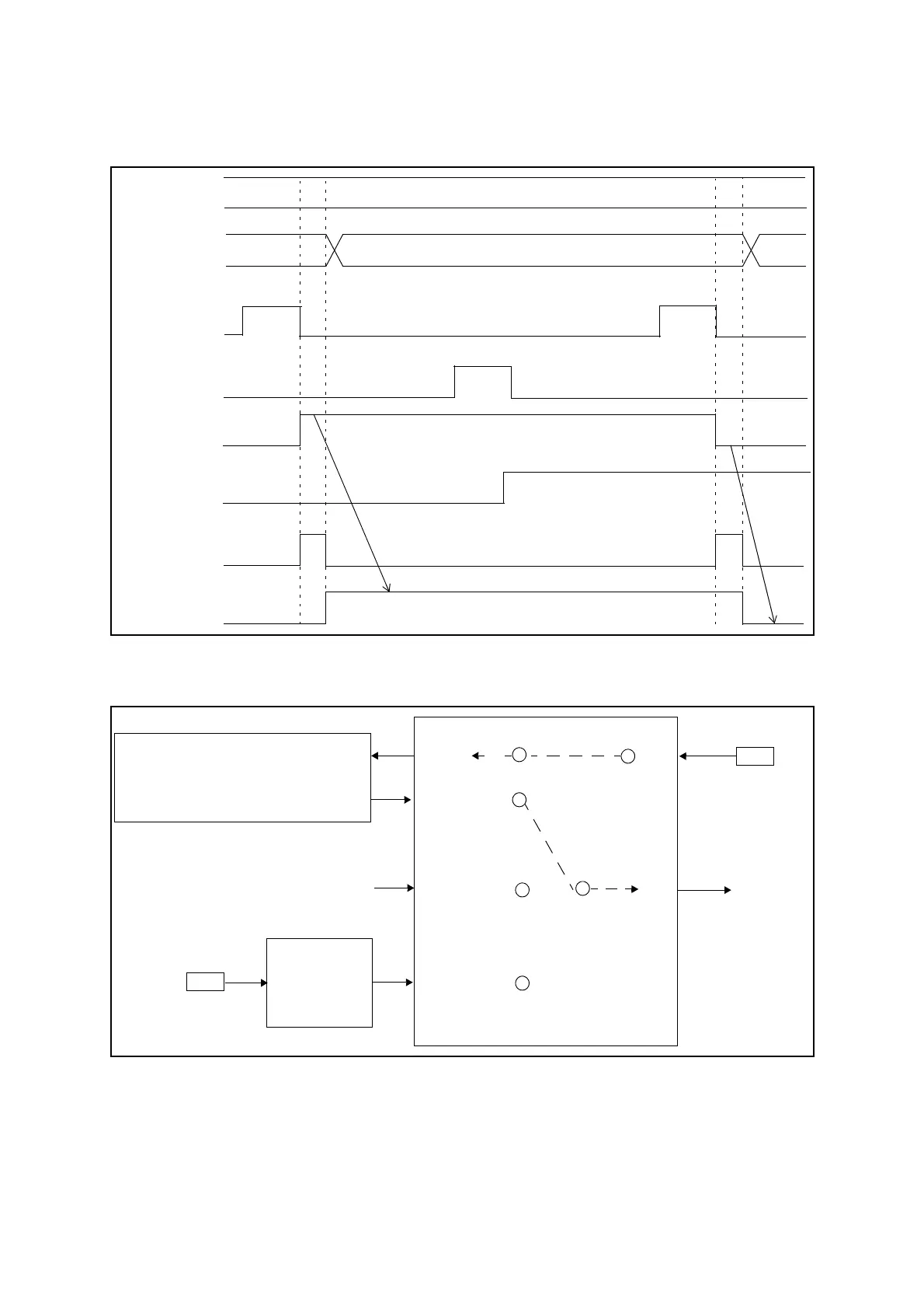
■ OPDUR and OPDLR Write Timing Diagram (OPS[2:0] = 0b000)
Figure 21.5-6 OPDUR and OPDLR Write Timing Diagram (OPS[2:0] = 0b000)
■ Signal Flow Diagram for Reload Timer Underflow by Setting OPS[2:0] = 0b001
Figure 21.5-7 Signal Flow Diagram for Reload Timer Underflow (OPS[2:0] = 0b001)
The 16-bit reload timer can be started by TIN input or a software trigger. The write signal is
controlled by the 16-bit reload timer underflow.
OPS[2:0]
WTO
0b000
ODBR1W
RDA[2:0]
ODBR0W
OPDBRL0[0]
0b001
0b101
OP00
OPDBRL1[0]
(OPDUR)
POSITION
16-BIT RELOAD TIMER
TIN
TOUT
DETECTION
TIN0O
WTIN0
WTIN1
WTO
TIN0
SNI2 to
TI1
WRITE
TIMING
DATA WRITE CONTROL UNIT
ODBR0W
OPDBRH0/OPDBRL0
OUTPUT
Pin
Pin
SNI0
WRITE SIGNAL