MB95630H Series
398 FUJITSU SEMICONDUCTOR LIMITED MN702-00009-2v0-E
CHAPTER 21 MULTI-PULSE GENERATOR
21.5 Operations
■ Signal Flow Diagram for Position Detection by Setting OPS[2:0] = 0b010 or
0b110
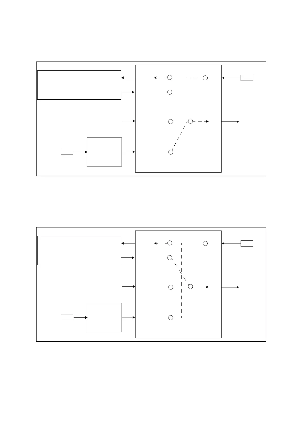
Figure 21.5-8 Signal Flow Diagram for Position Detection (OPS[2:0] = 0b010 or 0b110)
The write signal is generated by a comparison match or effective edge input of position
detection.
■ Signal Flow Diagram for Reload Timer and Position Detection by Setting
OPS[2:0] = 0b011 or 0b111
Figure 21.5-9 Signal Flow Diagram for Reload Timer & Position Detect
(OPS[2:0] = 0b011 or 0b111)
At this setting the16-bit reload timer is started by the compare match or effective edge input of
the position detection circuit, write signal is then generated whenever the 16-bit reload timer is
underflow. The compare match is triggered by any effective edge change in SNI2 to SNI0 pins.
POSITION
16-BIT RELOAD TIMER
TIN
TOUT
DETECTION
TIN0O
WTIN0
WTIN1
WTO
TIN0
SNI2 to
TI1
WRITE
TIMING
DATA WRITE CONTROL UNIT
ODBR0W
OPDBRH0/OPDBRL0
OUTPUT
Pin
Pin
SNI0
WRITE SIGNAL
POSITION
16-BIT RELOAD TIMER
TIN
TOUT
DETECTION
TIN0O
WTIN0
WTIN1
WTO
TIN0
SNI2 to
TI1
WRITE
TIMING
DATA WRITE CONTROL UNIT
ODBR0W
OUTPUT
Pin
Pin
SNI0
OPDBRH0/OPDBRL0
WRITE SIGNAL