MB95630H Series
408 FUJITSU SEMICONDUCTOR LIMITED MN702-00009-2v0-E
CHAPTER 21 MULTI-PULSE GENERATOR
21.5 Operations
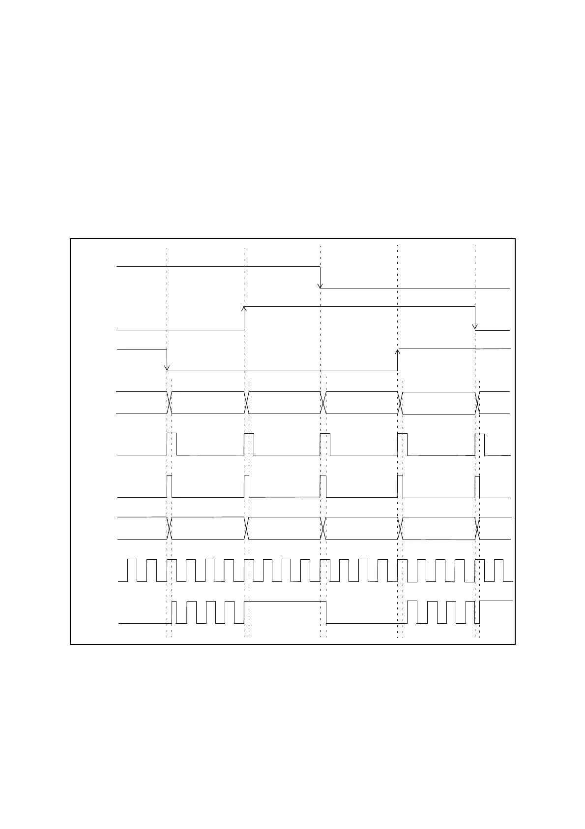
The comparisons between the SNI2 pin and the RDA2 bit, the SNI1 pin and the RDA1 bit, the
SNI0 pin and the RDA0 bit are done for each position detection.
The OPTx output waveform is updated according to the effective edge input to pin SNIx as
shown in Figure 21.5-17. The data of the 16-bit MPG output data buffer register (upper/lower)
(OPDBRHx/OPDBRLx) specified by the BNKF bit and the RDA[2:0] bits is transferred to the
16-bit MPG output data register (upper/lower) (OPDUR/OPDLR), and the output data is
renewed automatically when pins SNI2 to SNI0 are compared with the value of the RDA[2:0]
bits and matches.
The reload timer can be used in this operation mode.
■ Timing Generated by Position Detection (OPS[2:0] = 0b010)
Figure 21.5-17 Timing Generated by Position Detection (OPS[2:0] = 0b010)
OP0[1:0]
(OPDLR)
PPG
OPT0
0b010b00 0b11 0b00 0b10
0b1100b100 0b101 0b011 0b001
WTO
RDA[2:0]
(OPDUR)
SNI0
WTIN1
SNI1
SNI2
0b11