MB95630H Series
578 FUJITSU SEMICONDUCTOR LIMITED MN702-00009-2v0-E
CHAPTER 26 DUAL OPERATION FLASH MEMORY
26.8 Registers
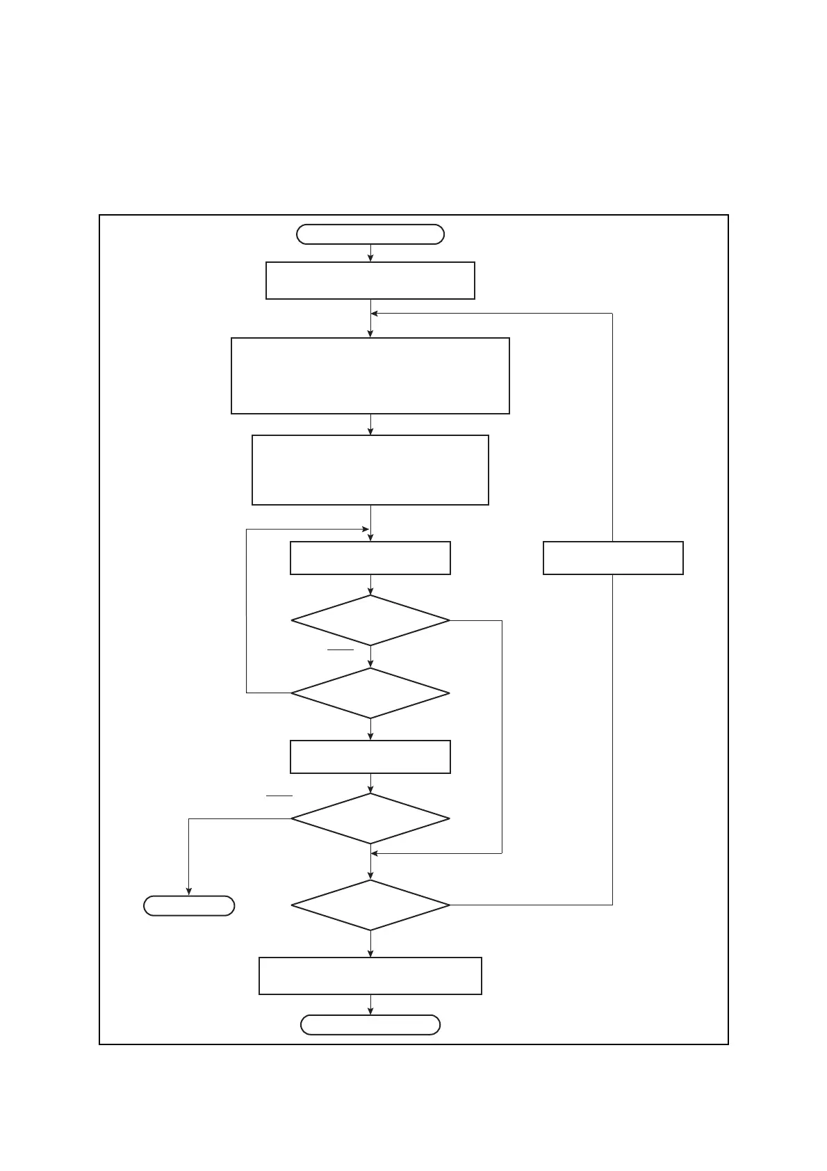
■ Flash Memory Sector Write Control Register 0 (SWRE0) Setup Flow Chart
Set the FSR:WRE bit to "1" to enable Flash memory programming, then enable or disable
programming data into a sector by setting the corresponding bit in the SWRE0 register to "1"
or "0" respectively.
Figure 26.8-13 Sample Procedure for Enabling/Disabling Flash Memory Programming
Start of programming
Read internal address.
Programming command sequence
(1) 0xUAAA ← 0xAA
(2) 0xU554 ← 0x55
(3) 0xUAAA ← 0xA0
(4) Program address ← Program data
Next address
Read internal address.
FSR:WRE
Enable Flash memory programming.
SWRE0
Enable/disable programming data to a sector.
(Write "0" to disable programming data or “1” to enable
programming data to a sector)
Data
Data
Execution timeout
(DQ5)
Data polling
(DQ7)
Data polling
(DQ7)
1
End of programming
0
Last address?
YES
NO
FSR:WRE
Disable Flash memory programming.
Program error
Data
Data