MB95630H Series
MN702-00009-2v0-E FUJITSU SEMICONDUCTOR LIMITED 621
APPENDIX A Instruction Overview
A.3 Bit Manipulation Instructions (SETB,
CLRB)
A.3 Bit Manipulation Instructions (SETB, CLRB)
Some peripheral function registers include bits that are read differently than
usual by a bit manipulation instruction.
■ Read-modify-write Operation
By using these bit manipulation instructions, you can set only the specified bit in a register or
RAM location to "1" (SETB) or clear to "0" (CLRB). However, as the CPU operates data in 8-
bit units, the actual operation (read-modify-write operation) involves a sequence of steps: 8-bit
data is read, the specified bit is changed, and the data is written back to the location at the
original address.
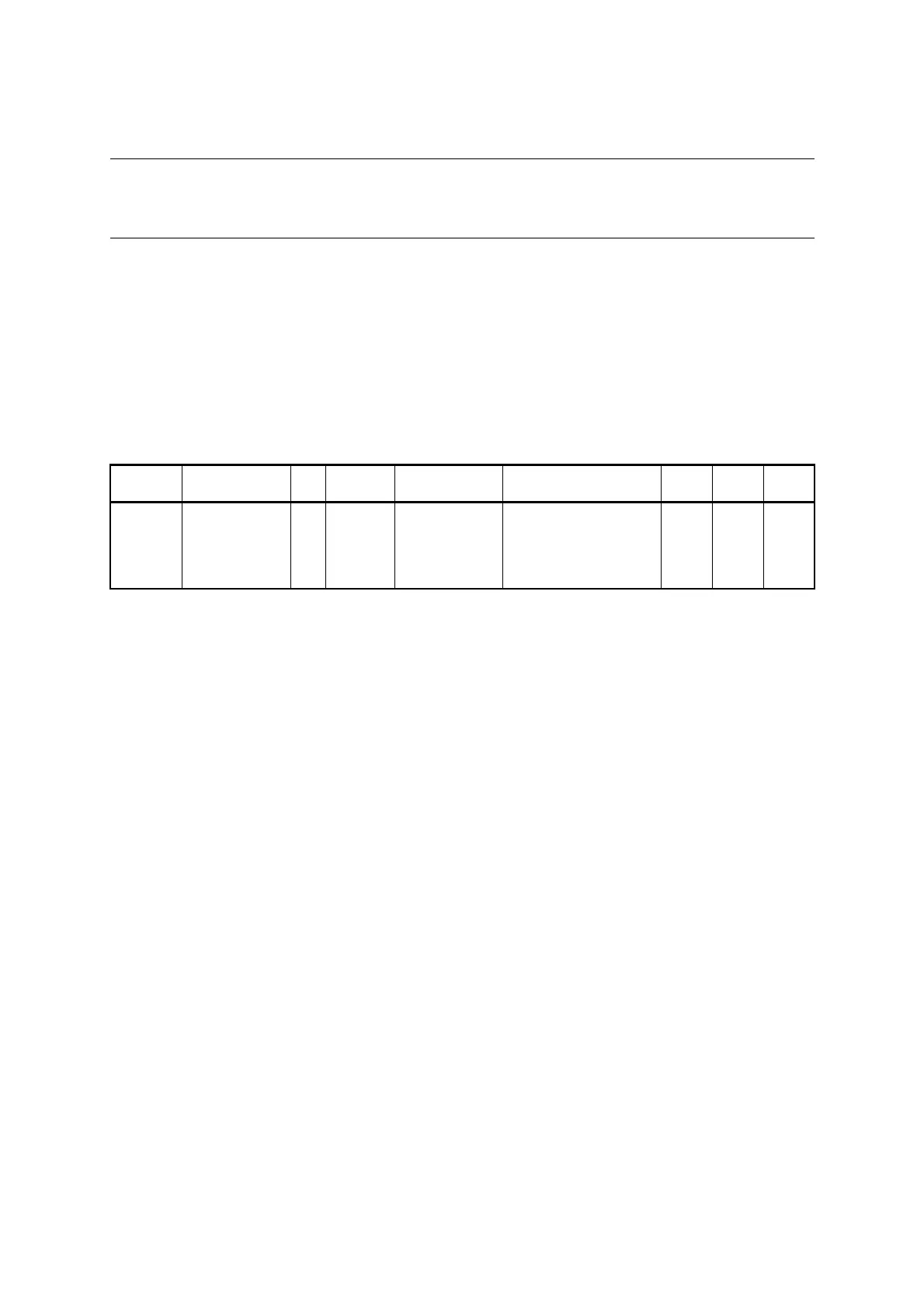
Table A.3-1 shows bus operation for bit manipulation instructions.
■ Read Destination on the Execution of Bit Manipulation Instructions
For some I/O ports and the interrupt request flag bits, the read destination differs between a
normal read operation and a read-modify-write operation.
● I/O ports (during a bit manipulation)
From some I/O ports, an I/O pin value is read during a normal read operation, while a port data
register value is read during a bit manipulation. This prevents the other port data register bits
from being changed accidentally, regardless of the I/O directions and states of the pins.
● Interrupt request flag bits (during a bit manipulation)
An interrupt request flag bit functions as a flag bit indicating whether an interrupt request
exists during a normal read operation, however, "1" is always read from this bit during a bit
manipulation. This prevents the flag from being cleared accidentally by writing the value "0" to
the interrupt request flag bit when manipulating another bit.
Table A.3-1 Bus Operation for Bit Manipulation Instructions
CODE MNEMONIC ~ Cycle Address bus Data bus RD WR RMW
A0 to A7
A8 to AF
CLRB dir:b
SETB dir:b
41
2
3
4
N+2
dir address
dir address
N+3
Next instruction
Data
Data
Instruction after next
1
1
0
1
0
0
1
0
1
1
0
0