MB95630H Series
46 FUJITSU SEMICONDUCTOR LIMITED MN702-00009-2v0-E
CHAPTER 3 CLOCK CONTROLLER
3.5 Operations in Low Power Consumption
Mode (Standby Mode)
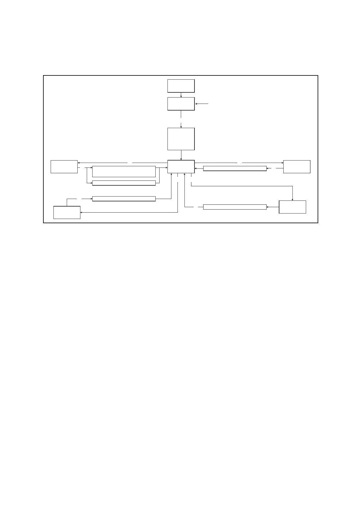
■ Standby Mode State Transition Diagram (with Deep Standby Mode Enabled)
Figure 3.5-2 shows a standby mode state transition diagram (with deep standby mode enabled).
Figure 3.5-2 Standby Mode State Transition Diagram (with Deep Standby Mode Enabled)
*: Flash memory recovery wait time (SCLK: source clock, MCLK: machine clock)
• In main clock mode, main CR clock mode, or main CR PLL clock mode
Maximum: 10 SCLK + 150 µs + 6 MCLK
• In subclock mode or sub-CR clock mode
Maximum: 2 SCLK + 150 µs + 6 MCLK
Power on
Reset state
Normal
(RUN) state
Watch mode
Main clock/main CR clock/main CR PLL clock/
subclock/sub-CR clock
oscillation stabilization wait time
Sleep mode (Flash recovery wait time*)
Sleep mode (Flash recovery wait time*)
Time-base
timer mode
Stop mode
Sleep mode
(1)
(2)
(3)
(5)
(6)
A reset occurs in any state.
<1>
(4)
(8)
(7)
Main CR clock
oscillation stabilization
wait time
+
sub-CR clock
oscillation stabilization
wait time
Sleep mode (Flash recovery wait time*)
Sleep mode (Flash recovery wait time*)