Section 2 CPU
Rev. 7.00 Mar 10, 2005 page 69 of 652
REJ09B0042-0700
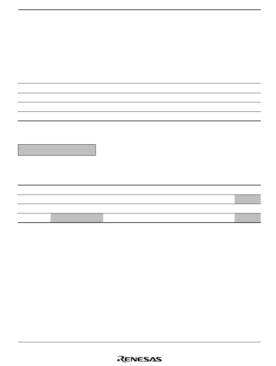
Example 2: BSET instruction executed designating port 3
P3
7
and P3
6
are designated as input pins, with a low-level signal input at P3
7
and a high-level
signal at P3
6
. The remaining pins, P3
5
to P3
1
, are output pins and output low-level signals. In this
example, the BSET instruction is used to change pin P3
0
to high-level output.
[A: Prior to executing BSET]
P3
7
P3
6
P3
5
P3
4
P3
3
P3
2
P3
1
P3
0
Input/output Input Input Output Output Output Output Output Output
Pin state Low level High level Low level Low level Low level Low level Low level Low level
PCR300111111
PDR310000000
[B: BSET instruction executed]
BSET #0 , @PDR3 The BSET instruction is executed designating port 3.
[C: After executing BSET]
P3
7
P3
6
P3
5
P3
4
P3
3
P3
2
P3
1
P3
0
Input/output Input Input Output Output Output Output Output Output
Pin state Low level High level Low level Low level Low level Low level Low level High level
PCR300111111
PDR3 0 1000001
[D: Explanation of how BSET operates]
When the BSET instruction is executed, first the CPU reads port 3.
Since P3
7
and P3
6
are input pins, the CPU reads the pin states (low-level and high-level input).
P3
5
to P3
0
are output pins, so the CPU reads the value in PDR3. In this example PDR3 has a value
of H'80, but the value read by the CPU is H'40.
Next, the CPU sets bit 0 of the read data to 1, changing the PDR3 data to H'41. Finally, the CPU
writes this value (H'41) to PDR3, completing execution of BSET.
As a result of this operation, bit 0 in PDR3 becomes 1, and P3
0
outputs a high-level signal.
However, bits 7 and 6 of PDR3 end up with different values.

 Loading...


