Section 6 ROM
Rev. 7.00 Mar 10, 2005 page 158 of 652
REJ09B0042-0700
6.5.4 Register Configuration
Table 6.5 lists the register configuration to control the flash memory when the built in flash
memory is effective.
Table 6.5 Register Configuration
Register Name Abbreviation R/W Initial Value Address
Flash memory control register 1 FLMCR1 R/W H'00 H'F020
Flash memory control register 2 FLMCR2 R H'00 H'F021
Flash memory power control register FLPWCR R/W H'00 H'F022
Erase block register EBR R/W H'00 H'F023
Flash memory enable register FENR R/W H'00 H'F02B
Note: FLMCR1, FLMCR2, FLPWCR, EBR, and FENR are 8 bit registers. Only byte access is
enabled which are two-state access. These registers are dedicated to the product in which
flash memory is included. The product in which PROM or ROM is included does not have
these registers. When the corresponding address is read in these products, the value is
undefined. A write is disabled.
6.6 Descriptions of Registers of the Flash Memory
6.6.1 Flash Memory Control Register 1 (FLMCR1)
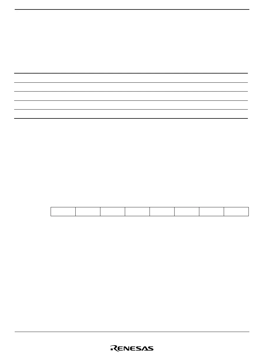
Bit 76543210
— SWE ESU PSU EV PV E P
Initial value 0 0 0 0 0 0 0 0
Read/Write — R/W R/W R/W R/W R/W R/W R/W
FLMCR1 is a register that makes the flash memory change to program mode, program-verify
mode, erase mode, or erase-verify mode. For details on register setting, refer to section 6.8, Flash
Memory Programming/Erasing. By setting this register, the flash memory enters program mode,
erase mode, program-verify mode, or erase-verify mode. Read the data in the state that bits 6 to 0
of this register are cleared when using flash memory as normal built-in ROM.
Bit 7—Reserved
This bit is always read as 0 and cannot be modified.

 Loading...


