Section 13 LCD Controller/Driver
Rev. 7.00 Mar 10, 2005 page 434 of 652
REJ09B0042-0700
Table 13.4 Power-Down Modes and Display Operation
Mode Reset Active Sleep Watch
Sub-
active
Sub-
sleep Standby
Module
Standby
Clock φ Runs Runs Runs Stops Stops Stops Stops Stops
*
4
φw Runs Runs Runs Runs Runs Runs Stops
*
1
Stops
*
4
ACT = 0 Stops Stops Stops Stops Stops Stops Stops
*
2
StopsDisplay
operation
ACT = 1 Stops Functions Functions Functions
*
3
Functions
*
3
Functions
*
3
Stops
*
2
Stops
Notes: 1. The subclock oscillator does not stop, but clock supply is halted.
2. The LCD drive power supply is turned off regardless of the setting of the PSW bit.
3. Display operation is performed only if φw, φw/2, or φw/4 is selected as the operating
clock.
4. The clock supplied to the LCD stops.
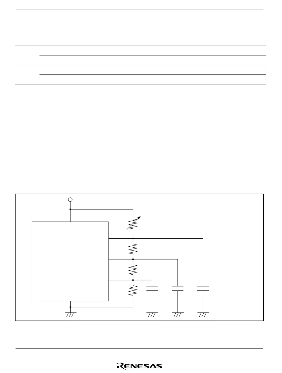
13.3.4 Boosting the LCD Drive Power Supply
When a large panel is driven, the on-chip power supply capacity may be insufficient. If the power
supply capacity is insufficient when V
CC
is used as the power supply, the power supply impedance
must be reduced. This can be done by connecting bypass capacitors of around 0.1 to 0.3 µF to
pins V
1
to V
3
, as shown in figure 13.9, or by adding a split-resistance externally.
This LSI
V
CC
V
SS
V
1
V
2
V
3
R
R
R
R = several kΩ to
several MΩ
C = 0.1 to 0.3 µF
R
Figure 13.9 Connection of External Split-Resistance

 Loading...


