Appendix C I/O Port Block Diagrams
Rev. 7.00 Mar 10, 2005 page 630 of 652
REJ09B0042-0700
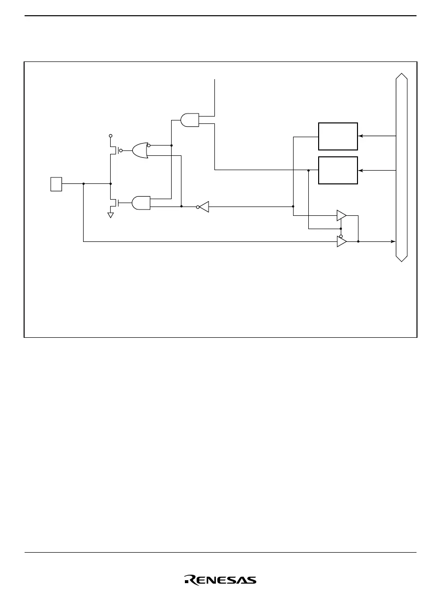
C.6 Block Diagram of Port 7
P7
n
V
CC
PDR7
n
Internal data bus
PCR7
n
SBY
V
SS
PDR7: Port data register 7
PCR7: Port control register 7
n = 7 to 0
Figure C.6 Port 7 Block Diagram

 Loading...


