Section 6 ROM
Rev. 7.00 Mar 10, 2005 page 162 of 652
REJ09B0042-0700
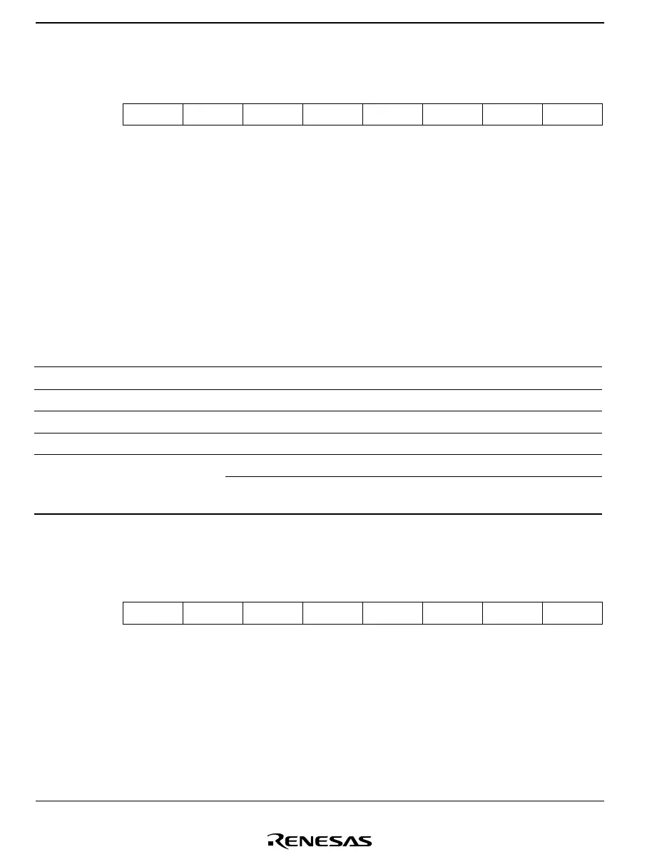
6.6.3 Erase Block Register (EBR)
Bit 76543210
— — — EB4 EB3 EB2 EB1 EB0
Initial value 0 0 0 0 0 0 0 0
Read/Write — — — R/W R/W R/W R/W R/W
EBR specifies the flash memory erase area block. EBR is initialized to H'00 when the SWE bit in
FLMCR1 is 0. Do not set more than one bit at a time, as this will cause all the bits in EBR to be
automatically cleared to 0. When each bit is set to 1 in EBR, the corresponding block can be
erased. Other blocks change to the erase-protection state. See table 6.6 for the method of dividing
blocks of the flash memory. When the whole bits are to be erased, erase them in turn in unit of a
block.
Table 6.6 Division of Blocks to Be Erased
EBR Bit Name Block (Size) Address
0 EB0 EB0 (1 Kbyte) H'0000 to H'03FF
1 EB1 EB1 (1 Kbyte) H'0400 to H'07FF
2 EB2 EB2 (1 Kbyte) H'0800 to H'0BFF
3 EB3 EB3 (1 Kbyte) H'0C00 to H'0FFF
4 EB4 EB4 (12 Kbytes) H'1000 to H'3FFF (HD64F38122)
EB4 (28 Kbytes)
H'1000 to H'7FFF (HD64F38124,
HD64F38024, HD64F38024R)
6.6.4 Flash Memory Power Control Register (FLPWCR)
Bit 76543210
PDWND———————
Initial value 0 0 0 0 0 0 0 0
Read/Write R/W — — — — — — —
FLPWCR enables or disables a transition to the flash memory power-down mode when the LSI
switches to subactive mode. The power supply circuit can be read in the subactive mode, although
it is partly halted in the power-down mode.

 Loading...


