Section 8 I/O Ports
Rev. 7.00 Mar 10, 2005 page 232 of 652
REJ09B0042-0700
8.9.3 Pin Functions
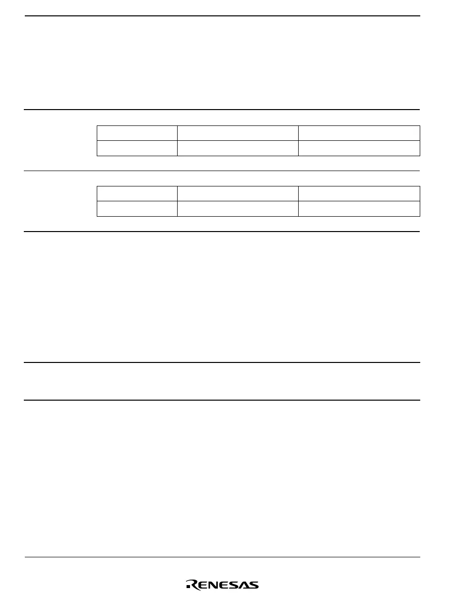
Table 8.24 shows the port 9 pin functions.
Table 8.24 Port 9 Pin Functions
Pin Pin Functions and Selection Method
P9
3
/V
ref
*
VREFSEL 0 1
Pin function P9
3
output pin V
ref
input pin
(n = 1 or 0)P9
1
/PWM
n+1
to
P9
0
/PWM
n+1
PMR9
n
01
Pin function P9
n
output pin PWM
n+1
output pin
Note: * The V
ref
pin is the input pin for the LVD’s external reference voltage. It is implemented on
the H8/38124 Group only.
8.9.4 Pin States
Table 8.25 shows the port 9 pin states in each operating mode.
Table 8.25 Port 9 Pin States
Pins Reset Sleep Subsleep Standby Watch Subactive Active
P9
5
to P9
2
P9
n
/PWM
n+1
to
P9
n
/PWM
n+1
High-
impedance
Retains
previous
state
Retains
previous
state
High-
impedance
Retains
previous
state
Functional Functional
(n = 1 or 0)

 Loading...


