Appendix B Internal I/O Registers
Rev. 7.00 Mar 10, 2005 page 555 of 652
REJ09B0042-0700
B.2 Functions
Bit
Initial value
R/W
7
0
W
6
0
W
5
0
W
4
0
W
3
0
W
2
0
W
1
0
W
0
TOLH CKSH2 CKSH1 CKSH0 TOLL CKSL2 CKSL1 CKSL0
0
W
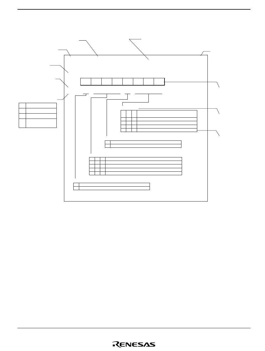
TCRFTimer Control Register F
H'B6
Timer F
Toggle output level L
Set to low level
Set to high level
16-bit mode, counts on TCFL overflow signal
Internal clock: φ/32
Internal clock: φ/16
Internal clock: φ/4
Internal clock: φ
w
/4
0
1
Toggle output level H
0
1
Set to low level
Set to high level
Clock select H
0
1
1
1
1
*
0
0
1
1
*
0
1
0
1
Counts on external event (TMIF) rising/
falling edge
Clock select L
1
1
1
1
0
0
1
1
0
1
0
1
Internal clock: φ/32
Internal clock: φ/16
Internal clock: φ/4
Internal clock: φ
w
/4
0 **
* Don't care
R
W
R/W
Read only
Write only
Read and write
See relevant register
description
Possible types of access
Initial bit values
Dashes () indicate
undefined bits.
Bit numbers
Register acronym
Register name
Address to which the register is mapped.
When displayed with two-digit number,
this indicates the lower address,
and the upper address is HFF.
Name of on-chip
supporting module
Names of the bits.
Dashes () indicate
reserved bits.
Full name of bit
Descriptions of bit
settings

 Loading...


