Section 4 Clock Pulse Generators
Rev. 7.00 Mar 10, 2005 page 105 of 652
REJ09B0042-0700
4.1.3 Register Descriptions
Table 4.1 lists the registers that control the clock pulse generators. The registers listed in table 4.1
are only implemented in the H8/38124 Group.
Table 4.1 Clock Pulse Generator Control Registers
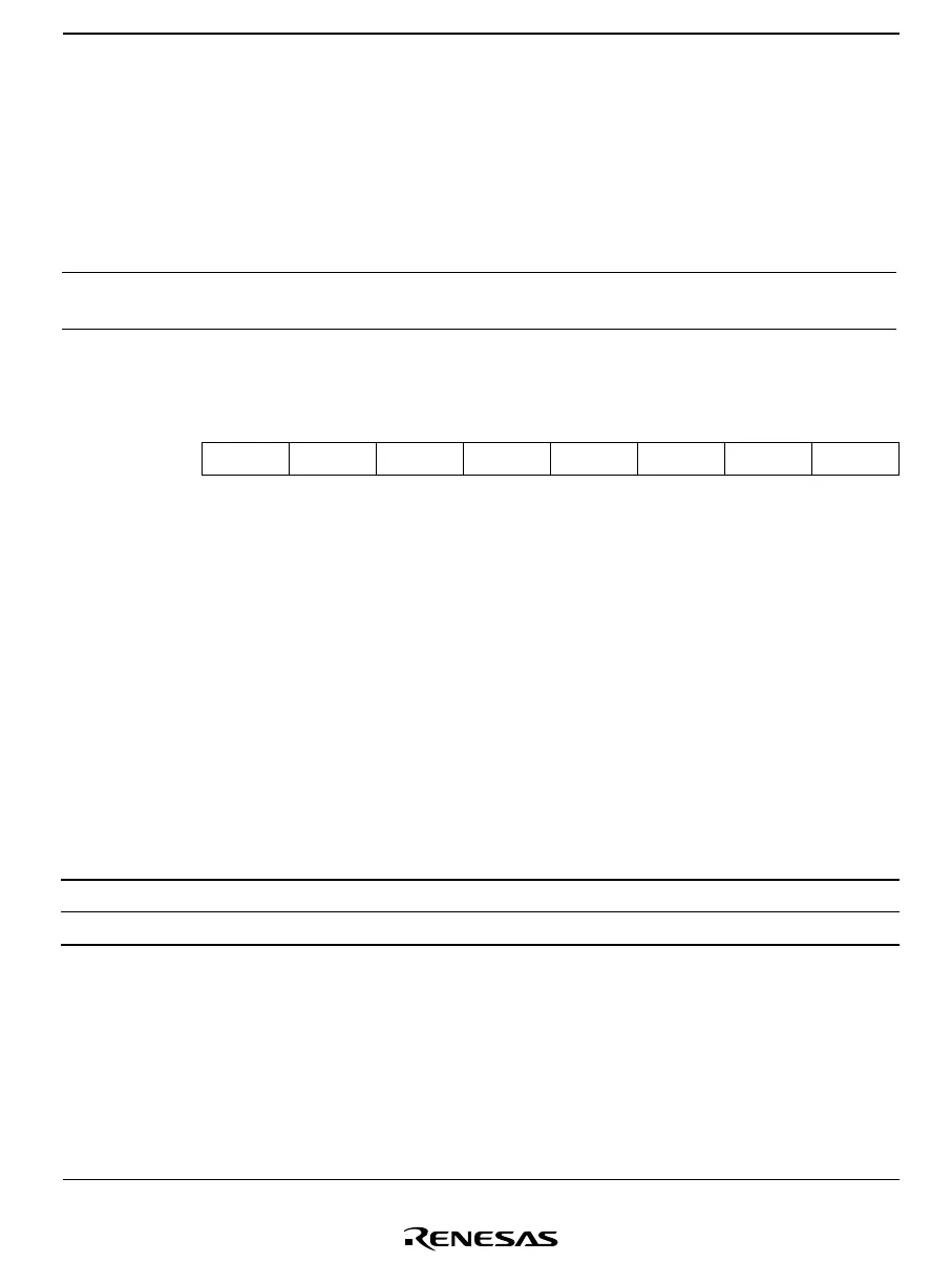
Name Abbreviation R/W Initial Value Address
Clock pulse generator control
register
OSCCR R/W — H'FFF5
Clock Pulse Generator Control Register (OSCCR)
Bit 76543210
SUBSTP — — — — IRQAECF OSCF —
Initial value 0 0 0 0 0 — — 0
Read/Write R/W R R/W R/W R/W R R R/W
OSCCR is an 8-bit read/write register that contains the flag indicating the selection of system
clock oscillator or on-chip oscillator, indicates the input level of the IRQAEC pin during resets,
and controls whether the subclock oscillator operates or not.
Bit 7—Subclock Oscillator Stop Control (SUBSTP)
Bit 7 controls whether the subclock oscillator operates or not. It can be set to 1 only in the active
mode (high-speed/medium-speed). Setting bit 7 to 1 in the subactive mode will cause the LSI to
stop operating.
Bit 7
SUBSTP Description
0 Subclock oscillator operates (initial value)
1 Subclock oscillator stopped
Bit 6—Reserved
This bit is reserved. It is always read as 0 and cannot be written to.
Bits 5 to 3—Reserved
These bits are read/write enabled reserved bits.

 Loading...


