Section 4 Clock Pulse Generators
Rev. 7.00 Mar 10, 2005 page 115 of 652
REJ09B0042-0700
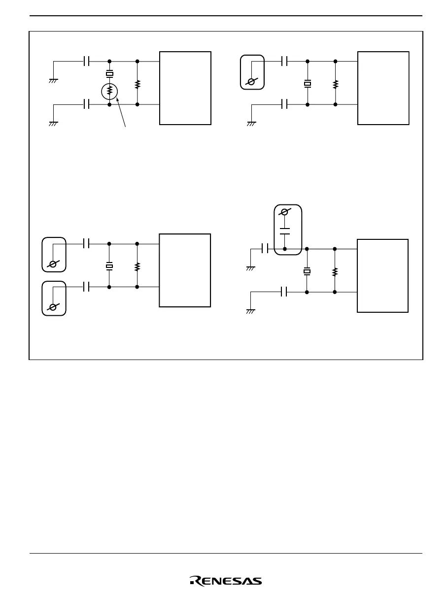
(1) Negative Resistance Measuring Circuit
(2) Oscillator Circuit Modification Suggestion 1
(3) Oscillator Circuit Modification Suggestion 2
(4) Oscillator Circuit Modification Suggestion 3
C3
OSC1
OSC2
Rf
C1
C2
Negative resistance,
addition of −R
OSC1
OSC2
Rf
C1
C2
Modification
point
Modification
point
Modification
point
OSC1
OSC2
Rf
C1
C2
OSC1
OSC2
Rf
C1
C2
Figure 4.13 Negative Resistance Measurement and Circuit Modification Suggestions
4.5.1 Definition of Oscillation Stabilization Wait Time
Figure 4.14 shows the oscillation waveform (OSC2), system clock (φ), and microcomputer
operating mode when a transition is made from standby mode, watch mode, or subactive mode, to
active (high-speed/medium-speed) mode, with an oscillator element connected to the system clock
oscillator.
As shown in figure 4.13, as the system clock oscillator is halted in standby mode, watch mode,
and subactive mode, when a transition is made to active (high-speed/medium-speed) mode, the
sum of the following two times (oscillation stabilization time and wait time) is required.

 Loading...


