Section 16 Electrical Characteristics
Rev. 7.00 Mar 10, 2005 page 519 of 652
REJ09B0042-0700
16.8.3 AC Characteristics
Table 16.22 lists the control signal timing and table 16.23 lists the serial interface timing.
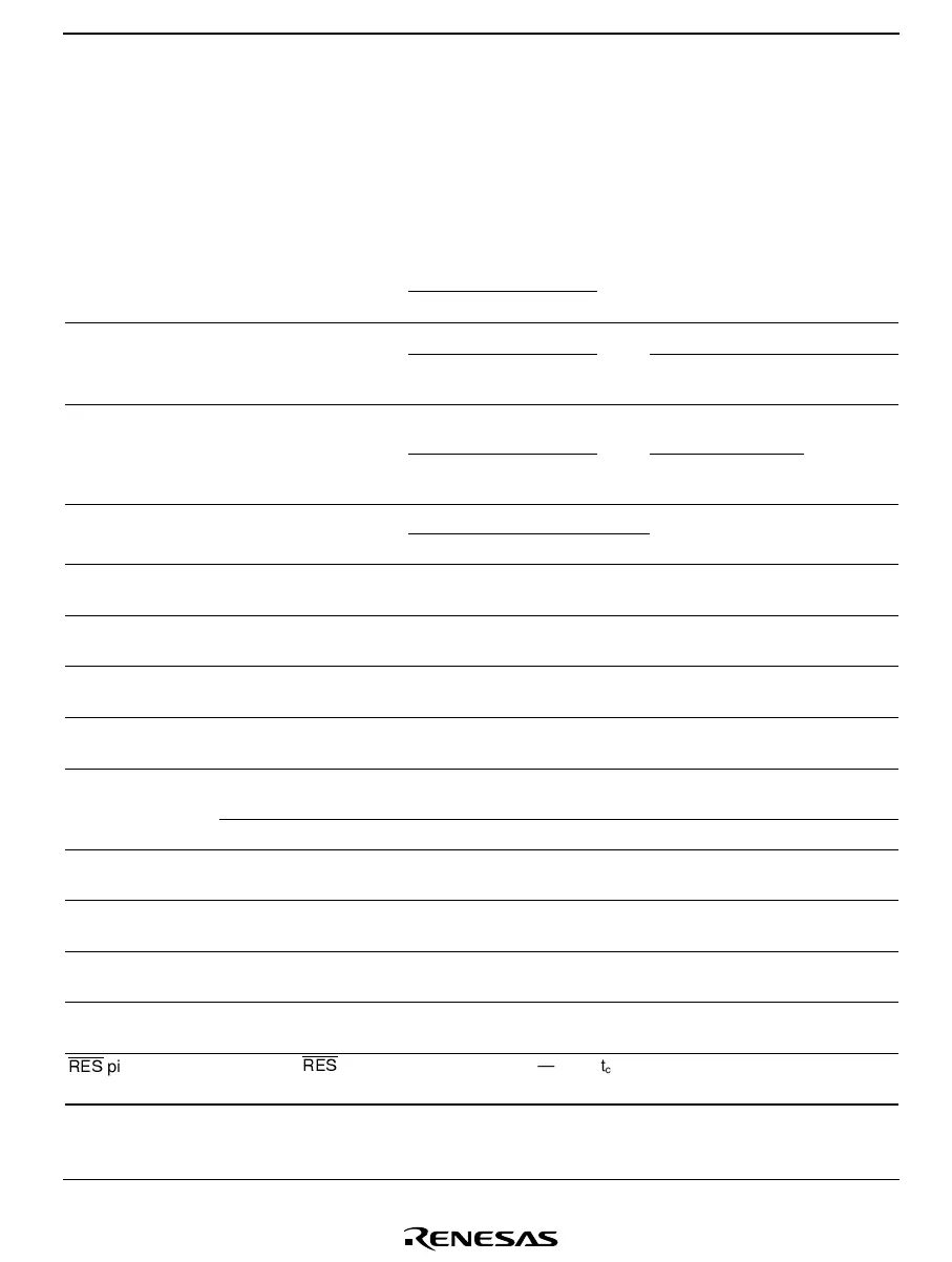
Table 16.22 Control Signal Timing
V
CC
= 2.7 V to 5.5 V, AV
CC
= 2.7 V to 5.5 V, V
SS
= AV
SS
= 0.0 V, unless otherwise specified
Values
Item Symbol
Applicable
Pins Min Typ Max Unit Test Condition
Reference
Figure
f
OSC
OSC
1
, OSC
2
2.0 — 20.0
MHz
System clock
oscillation
frequency
0.7
— 2.0 On-chip oscillator
selected
*
2
OSC clock (φ
OSC
)
cycle time
t
OSC
OSC
1
, OSC
2
50.0 — 500
ns
Figure 16.1
500
— 1429 On-chip oscillator
selected
t
cyc
2— 128t
OSC
System clock (φ)
cycle time
—— 182µs
Subclock oscillation
frequency
f
W
X
1
, X
2
— 32.768 — kHz
Watch clock (φ
W
)
cycle time
t
W
X
1
, X
2
— 30.5 — µs Figure 16.1
Subclock (φ
SUB
)
cycle time
t
subcyc
2— 8 t
W
*
1
Instruction cycle
time
2— — t
cyc
t
subcyc
Oscillation
stabilization time
t
rc
OSC
1
,
OSC
2
—— 20 ms
t
rc
X
1
, X
2
—— 2.0 s
External clock high
width
t
CPH
OSC
1
20 — — ns Figure 16.1
External clock low
width
t
CPL
OSC
1
20 — — ns Figure 16.1
External clock rise
time
t
CPr
OSC
1
— — 5 ns Figure 16.1
External clock fall
time
t
CPf
OSC
1
— — 5 ns Figure 16.1
RES
pin low
width
t
REL
RES
10 — — t
cyc
Figure 16.2

 Loading...


