Section 12 A/D Converter
Rev. 7.00 Mar 10, 2005 page 405 of 652
REJ09B0042-0700
Bit 7—A/D Start Flag (ADSF)
Bit 7 controls and indicates the start and end of A/D conversion.
Bit 7
ADSF Description
0 Read: Indicates the completion of A/D conversion (initial value)
Write: Stops A/D conversion
1 Read: Indicates A/D conversion in progress
Write: Starts A/D conversion
Bits 6 to 0—Reserved
Bits 6 to 0 are reserved; they are always read as 1, and cannot be modified.
12.2.4 Clock Stop Register 1 (CKSTPR1)
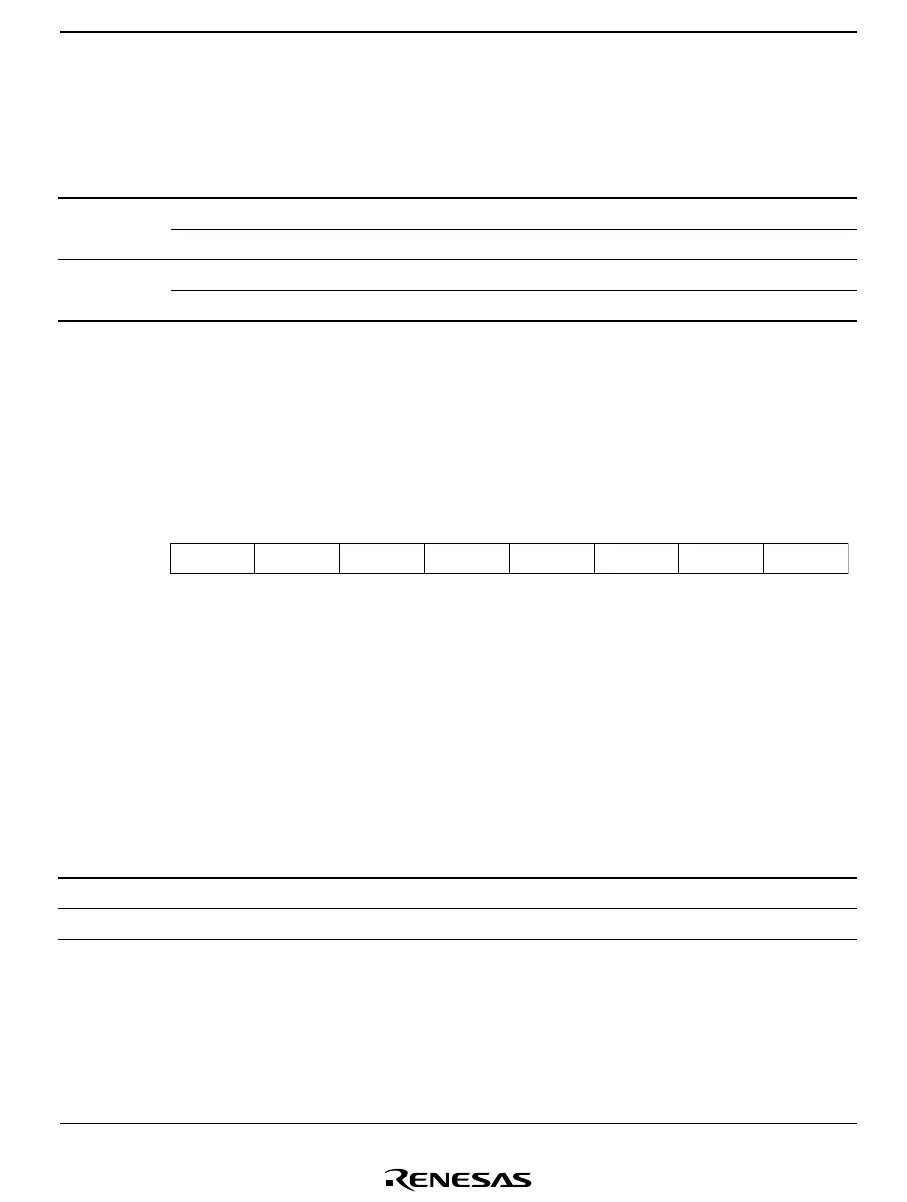
TFCKSTP TCCKSTP TACKSTP S32CKSTP ADCKSTP TGCKSTP
76543210
1
1111111
R/W R/W R/W
R/W R/W
R/W
Bit
Initial value
Read/Write
CKSTPR1 is an 8-bit read/write register that performs module standby mode control for peripheral
modules. Only the bit relating to the A/D converter is described here. For details of the other bits,
see the sections on the relevant modules.
Bit 4—A/D Converter Module Standby Mode Control (ADCKSTP)
Bit 4 controls setting and clearing of module standby mode for the A/D converter.
ADCKSTP Description
0 A/D converter is set to module standby mode
1 A/D converter module standby mode is cleared (initial value)

 Loading...


