Section 2 CPU
Rev. 7.00 Mar 10, 2005 page 55 of 652
REJ09B0042-0700
2.6 Basic Operational Timing
CPU operation is synchronized by a system clock (φ) or a subclock (φ
SUB
). For details on these
clock signals see section 4, Clock Pulse Generators. The period from a rising edge of φ or φ
SUB
to
the next rising edge is called one state. A bus cycle consists of two states or three states. The
cycle differs depending on whether access is to on-chip memory or to on-chip peripheral modules.
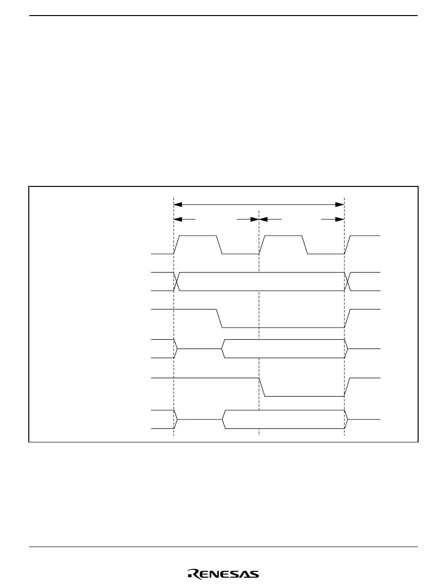
2.6.1 Access to On-Chip Memory (RAM, ROM)
Access to on-chip memory takes place in two states. The data bus width is 16 bits, allowing
access in byte or word size. Figure 2.11 shows the on-chip memory access cycle.
T
1
state
Bus cycle
T
2
state
Internal address bus
Internal read signal
Internal data bus
(read access)
Internal write signal
Read data
Address
Write data
Internal data bus
(write access)
φ or φ
SUB
Figure 2.11 On-Chip Memory Access Cycle

 Loading...


